EEVblog #532 - Silicon Chip Wafer Fab Mailbag

preview_player
Показать описание
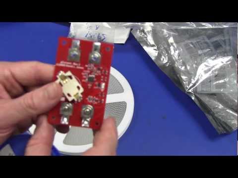
A look at some equipment and wafers used in the manufacture of silicon chip wafers.
200mm and 300mm wafers, die, dice sawing, lead-frame manufacture, automated testing machine (ATE) probing, clean room bunnie suits, photo plots, BGA chip thermal test sockets, and the worlds smallest active FET probes at 100 nanometers for direct wafer probing!
Thanks to Vincent Himpe:

EEVblog Main Web Site:
EEVblog Amazon Store:
Donations:
Projects:
Electronics Info Wiki:
Рекомендации по теме
Комментарии
Автор

As a retired test engineer working at National Semi, Motorola and other semi houses here's a couple tidbits about wafer probing.

First, the probe card does not move, all motion is in the chuck that holds the wafer using vacuum. The chuck is positioned in X, Y and Z by linear motors in the most common Electroglas probers. The pcb is very thick because probing high pin count die requires an extremly rigid material to withstand the significant amounts of force needed to deflect the probes such that they all make contact. This Z axis distance is in the order of 1 to 3 thousandths of an inch.

Second, the probe ring is mated to the pcb after it is assembled on precision fixturing to position the tip of each probe in the center of the die bond pad and perfectly aligned in Z axis. Once the probes are positioned the assembly is encapsulated in an epoxy ring, hence the name "epoxy ring probe card". The probes are tungsten which has the necessary mechanical and electrical properties required. Probe cards are periodically "aligned and planarized" after probing 25 to 100 wafers and to repair damage. This is done by highly skilled technicians under a microscope.

Hopes this is helpful. Probing technology has come a long way since the 60's when I first used them.

demyhr
Автор

In 1976 Harris Semiconductor in Melbourne, Fl. gave me the .50 tour as to how they made their silicon chips. Pretty remarkable especially back then.

WINCHESTER
Автор

Beautiful wafers....I remember when i was in Elementary and on "career" day this geeky guy brought a wafer to show us and try his best to explain what they are and why they were so important and how in the future they would get more complex....this was about 20 years ago and I just can't believe how beautiful they are and AMAZING...wish I could go back in time and admire the wafer.

No one paid attention to that geek, everyone wanted to see the stupid cop or firefighter. LOL.

jeanious
Автор

Just looking at some of these older vids. Here's a story I heard years ago about a chip fabrication factory.

Once the circuit lines have been etched onto the chips, the chips pass through a kiln to harden the circuit lines on the silicon. The kilns were similar to those pizza ovens that have a conveyor belt in them, cold pizza goes in one side and hot pizza comes out the other side.

There was a chip factory (I never heard exactly which one) where the defect rate of the chips would mysteriously skyrocket once in a while, then go back to normal, only to skyrocket again a few weeks later again. The engineers at the factory were tearing their hair out trying to find the cause of the defect surges.

One Friday evening one of the engineers was working back late and as he was on his way out he went past the chip kiln area and found some of the night shift workers had been putting frozen pizzas through the chip kiln as a late night snack. Fat and other substances from the pizzas were then contaminating the sets of chips that went through the kiln after the pizzas had been cooked, causing the defect rate for the chips to suddenly rise. A bunch of people in the factory suddenly became unemployed.

garethbull
Автор

At around the 38:00 minute mark, those are not pinholes that he is seeing through the probe. Those are the reflections of his camera's LED lights. The LEDs are reflecting from the glassy surface of the probe material.

spayderninja
Автор

Those wafers are insane, the level of detail and scale is ridiculous. Very interesting and demonstrated how little I know about processor architecture! Thanks for posting.

stoatythesecond
Автор

The semi industry is divided into back-end and front-end operations. The back-end  - cutting, testing etc - is usually done in the far east. The front-end is the actual fabrication process which involves lithography, etch, furnace, sputter and implant -  virtually all use  robotics to handle the wafers. The actual fabrication process can take up to 6 weeks and the wafer might have up to a dozen layers. 

Sabhail_ar_Alba
Автор

38:28 They're not pinholes. It's the reflection of the microscope LED.

shreyasrao
Автор

so cool. by bar, chip manufacturing is one of the most, if not THE most amazing production technologies we have developed.

It's crazy to. Moores law is just sloing down now.

pattyoneill
Автор

I kept avoiding this video thinking that the video was going to be about chip reels. Much more interesting than expected. Keep up the good work. Thank you for sharing this with us.

tjay
Автор

Vincent Himpe thank you so much to be so gracious supplying these FAB parts. Marvelous : - ))

abpccpba
Автор

Hi Dave
A few small corrections from a wafer sort person.
If you look close on the probe card you noted that some some of the probes were shorted. Those pins are power pins Vcc or Gnd supply's .

The next comment is that the probe card does not come down on the pins the wafer moves under the probe.


the probe card you have is the xyz accuracy of such a probe card the height diffrence between the first and last pin needs to be >5 mil


ArieLash
Автор

the probe card had 144 wires on each side of the square just in case anyone was wondering
PS i counted this at 3am so i may be a little off ^-^

shark
Автор

Great example of some unbelievably microscopic work that goes on behind the scenes to provide us with modern semiconductor components. Thanks for sharing.

van-c
Автор

This is so interesting. I have no idea what I'm watching.

spaceframe
Автор

I used to work at the IBM 200mm fab in Burlington Vermont USA and we used to call the cleanroom suits, graph paper ninjas. Had to share. I also used to take home the old reticles for the photolithography Nikon tools. I wish I still had some because I would send one too you. Uber cool looking.

numberpirate
Автор

just finds this EEVblog videos...pure gold dude.

emem
Автор

Oh I want to get a full wafer so badly one day. They are absolutely stunning to see.

Zenodilodon
Автор

Damn that interesting, thank you Vincent all these years on.

Paul--W
Автор

Thanks for posting, I've worked in the industry for many years but never had an overview like this before.

carabela
visit shbcf.ru