EEVblog #239 - PCB Design For Manufacture Part 2
preview_player
Показать описание
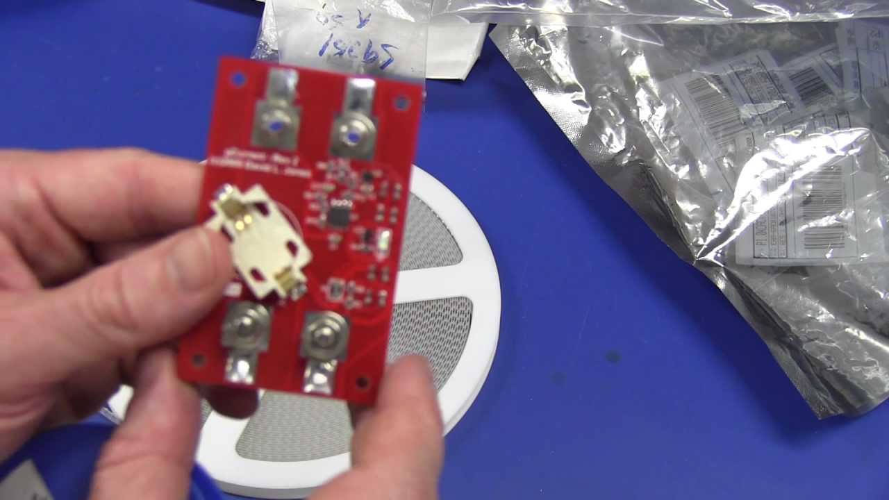
A follow up to Dave's popular PCB Design For Manufacture (DFM) tutorial video.
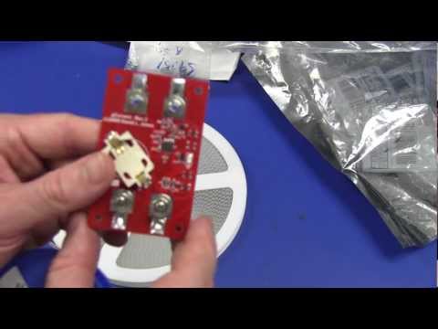
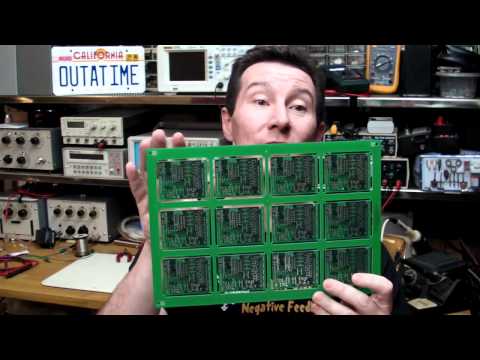
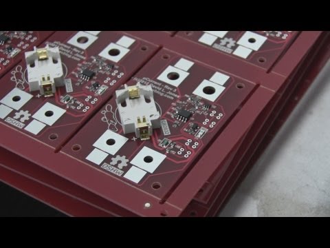
This time he updates his uCurrent PCB for production, including panelisation layout and component reel selection. Lots of the same ground is covered as in part 1, but with a specific real project example.
Рекомендации по теме
Комментарии
Автор

@valajbeg This is non-scripted stream-of-consciousness stuff. I do not realise how much I'm saying or how often I repeat things or say umm or mumble until I go to edit all the clips. If it's too long then I'm not going to go back and re-shoot for succinctness. If I did that then I'd never get any videos out.

EEVblog
Автор

This series is exactly the stuff I want to know that my college doesn't teach and that I can barely find information online for the common / standardized details and such. Thank you IMMENSELY for sharing all of your knowledge in SUCH specific detail and insight.

autofigure
Автор

While watching this, a thought occurred to me. There is another cost that you didn't include for high volume production. Storage! You can't expect to make 10, 000 boards and just stick them in your bedroom closet or something, you have to have somewhere to put them. If there are enough of them, you may even need to rent space in a warehouse or something.

I doubt most viewers are in the range where storage becomes a significant issue, but it just popped into my head while watching this.

magicphysicsdude
Автор

You are like the blue's clues of the ecad world. Can't stop watching.

AdityaGaddam
Автор

Oh Boy, DAVE YOU ARE brilliant, and a great man! Big strong handshake, for a such nice personality, and for disclosure very useful information in such details, especially useful for novices and dummies! Love You channel! It's like treasure for me.

mywebnet
Автор

@myshots101 I use the free package CamStudio and ensure that I have a fixed capture area of 1280x720, so it's exactly 16:9 format and does not need any manipulation in the video editor software.

EEVblog
Автор

@MickGalt You don't "snap" them, you lever them back and forth gently until they break.

EEVblog
Автор

@EEVblog Thank you. I thought I saw that but never used it. I got horrible lighting in my room apparently and my cheap point and shoot camera isn't much good indoors either. I also don't like to edit videos myself, they just take forever so whatever makes this less work is good for me.

myshots
Автор

I watched all of it and I love it. I think your industry-related videos are the best. This is very good info for me, as I started an apprenticeship on the R&D department of a local assembly house this week. Fantastic timing. :)

TheCrazyInventor
Автор

As for manufacture, have you considered using pick and place solder supplys in 0201, 0402, 0603, 0805 or 1206 formfactor so that you can have the entire board manufactured in a single reflow step, the manufacturer will use a temporary adhesive to the board and then all the through holw components can be made in the reflow oven, I think the technique is called pin and paste

The other technique is that you could design the board so that the SMT stuff is wave soldered.

varno
Автор

I've just watched almost two hours of your videos! Really enjoy your knowledge. I wish i understood 1/100th of what you're talking about.

enuro
Автор

@AnnoyingVerification That's adds up too. But pick and place can take a long time, much longer than paste application, depending upon the board complexity.

EEVblog
Автор

@fingerboy18 Usually done with an inkjet print of some sort. Not all manufacturers will offer that, gotta ask.

EEVblog
Автор

@blarque An automated jig for precision measurement like this is not trivial. You have to weight up how long it takes you to develop and build that vs how much time you save per unit. I wouldn't save much time, I have manual testing down pat and it's very quick.

EEVblog
Автор

Firstly, thanks for taking the time to make these & answering so many of the comments. Clearly you're helping a lot of people who know very little about PCB design & manufacture.

I might suggest though, rather than "PCB Design For Manufacture", you really should call these videos 'All About Board Panelization". In the hour of the first part, most of the time was spent talking about panelization, and in this one you spend another 40 minutes covering some of the same exact topics and there's very little discussion of board level layout techniques and constraints to make the PCB fab & assembly more reliable & repeatable. 
Speaking of a sign of an Engineer, so I don't fault you, but you repeat a LOT of things not only from the first video (probably because they're created 2 years apart), but multiple times in this video. You could've made this video half as long and thereby twice as helpful if you just made notes on what you wanted to cover and covered it once.

PrplhaZe
Автор

Yes it does. The panel is a just X copies of the main board file. Change the main bard file and all the panel boards change.

EEVblog
Автор

Do you have a video about the criteria you have to satisfy so that your designed circuits working properly after printing them on a board? For example I was thinking about topics like where to place your high and low voltage components in relation to electromagnetic compatibility and high frequency signals.

ulf
Автор

@mspeir The assembly process - parts can be lost when feeding the machine if the utmost care isn't taken, the machine can also drop parts - these are discarded. Likewise if the machine's cameras don't recognise the part for whatever reason the part is rejected.

turbochargedbrick
Автор

@MickGalt Unless you don't have one, in which case you can do it safely and easily by hand.

EEVblog
Автор

How do you get the PCBs and components to assembler though?

TheMiniProdigy