EEVblog #499 - What is JTAG and Boundary Scan?

preview_player
Показать описание
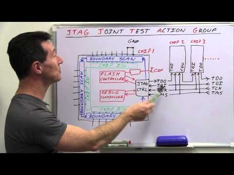
What is the JTAG interface and Boundary Scanning, how does it work, and what is it useful for?

EEVblog Main Web Site:
EEVblog Amazon Store:
Donations:
Projects:
Electronics Info Wiki:
Рекомендации по теме
Комментарии
Автор

I am software engineer with passion on hardware, used JTAG and ICE 10 years to bring up few products with fresh hw engrs passion on sw. We did. Now, the way you explaining things artistically can make any one understand and get motivated. Wow! Keep going for all.

babualluri
Автор

I realised that I wasted a whole day just theoritically googling to understand the jtag/boundary scan concept until I saw this video of yours <3 Thankkksss a lot for this. Your explanation was excellent . You deserve so much appreciation for giving such neatly explained videos :)

manjusha
Автор

wow! I have been using JTAG for programming for many years and I never realized about its true power until I saw this video! great work my friend!!!

matiasx
Автор

I always turn of adblocker when watching Daves channel. He deserves every penny he earns.

sologals
Автор

I have been working with electronics for a while, i have been hearing my colleagues using the word 'JTAG'... never knew what it meant or how it is used. this video was a great eye opener. words fall to short to describe the gratitude i have for such an insightful video thanks a million... keep up the good work man

frederickmkhombo
Автор

The real beauty of that xjtag system is that you can write code that describes how to test a particular chip. Once that's written, anytime you use the same chip on any of your boards you can call the same test routines. So it hides all the serial details from the user and makes your test routines very reusable. I loved it when I was doing test.

BoltClevo
Автор

We used JTAG to control uC. I never knew the "boundary scan" feature exists. Thank you for explaining the wonders of JTAG!

donmoore
Автор

You probably dont have time to read comments but you inspired me many years ago. I used to watch your videos knowing very little about this stuff. Today I'm repairing boards of all natures, doing trace repairs, and I've recently had to repair a completely snapped board. I was a software hacker, and hardware just seemed like the ultimate way to control and manipulate hardware. During my time hardware hacking I invested in a good stereo microscope, oscilloscope and rework station. I had all the tools to do repairs, so now I do that because it's good money, more fun, and beats my old programming career. Thank you :D

JayJay-kimi
Автор

EEVblog  Thank you so much for these videos! As an engineering student with a lot of interest in electronics, I have been watching your videos quite often, and always learn something new! Thanks again Dave!

Brokenrocktail
Автор

Well yes, of course you need good software to decode all display the info, otherwise you are just looking at The Matrix

EEVblog
Автор

Thought JTAG was difficult
But you forced me to change my mind.
Thank you very much

shreyashpatil
Автор

You are better than the best professor at my college. Great video. Keep up the great work. The electronics world needs more people like you!

MohammedNoorSK
Автор

Nobody can equal Dave when explaining difficult subjects like this and make them easy to understand!

stm
Автор

Wow, I normally have a difficult time understanding hardware related stuff, but you explain it like it was basic.
It takes an expert to explain difficult stuff easy. You nailed it, subscribed.

philipschroeder
Автор

One of the best (if not the best) explanation of JTAG and Boundary Scanning that I've seen. Good stuff. 

murrij
Автор

@AvstoMusic - Each JTAG pin "site" knows whether it's an input or not, so an input won't 'adopt' its shifted-in value. Instead, it will ignore the shifted-in value and shift out its current value - when TMS is strobed, at least! So a host performs a complete scan by: [1] Shifting N bit values; [2] Strobe TMS to "Make It So!" (see my previous comment); [3] Shifting N bit values. That will program the outputs to the desired values, and then read the resultant values.

johnadriaan
Автор

Excellent explanation of 1149.1 Boundary Scan, but if the green rectangles represent your I/O driver & receiver ckts, then I would have drawn the the green rectangles outside of the blue ones. The output test data is fed into the drivers by scanning it into the boundary scan latches and then driven off-chip. The receivers conversely receive input test data from off-chip and feed it into the boundary scan latches, where it is captured and scanned out. As drawn, this diagram implies that latching occurs between I/O ckts and the physical chip pin.

briankessler
Автор

Found it in 2022. This is an amazingly clear explanation! Thank you so much. Really helps one understand what the heck JTAG is.

affinitystablepeanuts
Автор

If you're hacking/reverse engineering a PCB that doesn't have an obvious JTAG connector (but suspect it's still there based on the chips on-board), you can use something like the JTAGulator, which is an open source tool I recently designed. Just connect to test points on the target board and have the tool try to determine if a JTAG interface actually exists. Once you've determined the pinout, you can use standard JTAG tools to start interfacing directly with the chips, extract firmware, etc.

JoeGrand
Автор

I always use the lapel mic for recording FF video, I have to, as the camera is 3 meters away. But when shooting on the bench I use the internal mic.
Lapel mics are not perfect, and if you turn your head the volume varies a lot. I passed this one through The Levelator to level out the audio, which is not easy to do in my Sony video editing software.

EEVblog