filmov
tv
EEVblog #1176 - 2 Layer vs 4 Layer PCB EMC TESTED!

Показать описание
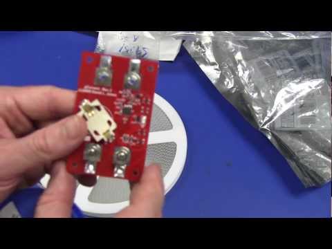
What difference does a 4 layer PCB make to EMC radiated emissions compared to an identical 2 layer PCB? And why?
Dave does H-Field near-field probe testing on two otherwise identical PCB's.
Electromagnetic waves and the difference between near field and far field, and H-Field and E-field probes and wave impedance is also explained.
The PCB layout is then examined to look at loop area and by-passing and what effect this has.
Bitcoin Donations: 38y7DE8HEHNj8fGDtUr4PkCn9nWxiorvvy
Litecoin: ML7oQokTwB38bgzzjLDbRV97HKAHuwRfHA
Ethereum: 0x11AceA38DCA9DbFfB4F35f3F746af65F9dED28ce
Support the EEVblog through Patreon!
Buy anything through that link and Dave gets a commission at no cost to you.
Stuff I recommend:
Donate With Bitcoin & Other Crypto Currencies!
#PCBdesign #PCBdesign #EMC
 0:36:21
EEVblog #1176 - 2 Layer vs 4 Layer PCB EMC TESTED!
 0:56:54
EEVblog #239 - PCB Design For Manufacture Part 2
 0:00:59
Always Have a Side Hustle
 0:37:29
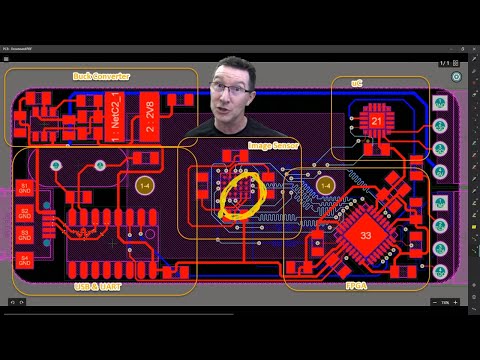
EEVblog #1323 - PCB Layout Review & Analysis
 0:00:35
I Was A Document God
 0:27:03
EEVblog #1327 - 3 Ways to FAIL at PCB Manufacture
 0:29:42
EEVblog 1559 - PCB Design: Trace Current Rating
 0:10:40
6 Horribly Common PCB Design Mistakes
 0:16:25
EEVblog #1273 - EMC Near Field vs Far Field Explained
 0:29:57
EEVblog 1430 - Rent vs Buy - My $400,000 MISTAKE!
 0:19:51
EEVblog #1157 - Transistor Zener Clamp Circuit
 0:35:07
EEVblog #1081 - Are Bypass Capacitors REALLY needed?
 0:30:46
EEVblog #1117 - PCB Power Plane Capacitance
 0:39:34
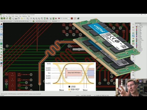
EEVblog #1247 - DDR Memory PCB Propagation Delay & Layout
 0:00:27
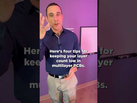
4 Strategies to Keep Your PCB Layer Count Low #pcbdesign #electronics #altium
 0:55:19
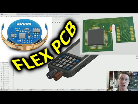
EEVblog #1262 - Designing a Flex PCB + uSupply Update
 0:18:02
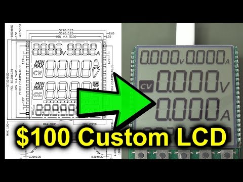
EEVblog #1105 - $100 Custom LCD Design - Part 3 (µSupply Part 18)
 0:29:49
EEVblog #1132 - The 3 Cent Microcontroller!
 0:25:10
EEVblog #469 - Cockcroft-Walton Multiplier
 0:18:49
eevBLAB #60 - Kickstarter Free Energy SCAMS!
 0:35:53
EEVblog #1180 - Component Parametric Search Tutorial
 0:36:13
EEVblog #1179 - Mailbag
 0:18:42
EEVblog #730 - Thin Film Resistor Networks
 0:17:40
EEVblog #1170 - TRUE Mystery Teardown! (not even Dave knows)
Комментарии