filmov
tv
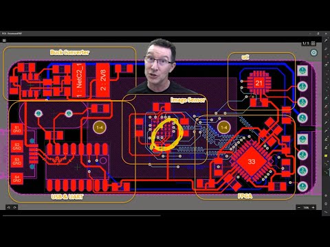
EEVblog #1323 - PCB Layout Review & Analysis

Показать описание
Dave analyses a PCB layout from the EEVblog forum and covers all sorts of tips for SMD layout, component placement, routing, layer stackup, controlled impedance traces, supply planes and power bypassing.
#PCB #Design #Tutorial
Support the EEVblog through Patreon!
Buy anything through that link and Dave gets a commission at no cost to you.
Donate With Bitcoin & Other Crypto Currencies!
#PCB #Design #Tutorial
Support the EEVblog through Patreon!
Buy anything through that link and Dave gets a commission at no cost to you.
Donate With Bitcoin & Other Crypto Currencies!
 0:37:29
EEVblog #1323 - PCB Layout Review & Analysis
 0:27:03
EEVblog #1327 - 3 Ways to FAIL at PCB Manufacture
 0:56:54
EEVblog #239 - PCB Design For Manufacture Part 2
 0:19:48
EEVblog #1373 - DIY PCB Photograhy LED Light Box - Part 2
 0:00:59
The Problem With Tech Media - STOP IT!
 0:29:42
EEVblog 1559 - PCB Design: Trace Current Rating
 2:13:23
LIVE KiCAD 5 PCB Design
 0:19:35
EEVblog #1372 - DIY PCB Photography Light Box
 0:00:59
Always Have a Side Hustle
 0:42:31
EEVblog #990 - Getting The PCB Manufactured (Nixie PART 5)
 0:45:10
EEVblog #1365 - Viewer PCB & Circuit Design Review
 0:23:04
EEVblog #1328 - uCurrent OPA189 Measurements
 0:10:40
6 Horribly Common PCB Design Mistakes
 0:29:19
EEVblog #1325 - OPAMP Shootout - Datasheet Deep Dive
 0:47:45
EEVblog #1326 - How Engineering Minds Think Alike
 0:08:53
eevBLAB #78 - Engineering Student Job Advice
 0:01:00
EE Reacts to Tesla PCB Design | 1-Min Review
 0:29:51
EEVblog #1334 - Mystery Dumpster Teardown
 1:13:59
EEVblog #974 - PCB Layout Walkthrough - PART 4
 0:53:08
EEVblog #1318 - What's State-of-the-Art in µCurrent Opamps?
 0:14:43
Guest Video: Electronoobs - Building a POV Display
 0:00:34
pcb design course for all
 0:00:26
What are the guidelines of analog PCB layout?
 0:00:16
PCB design 2 layers #shorts
Комментарии