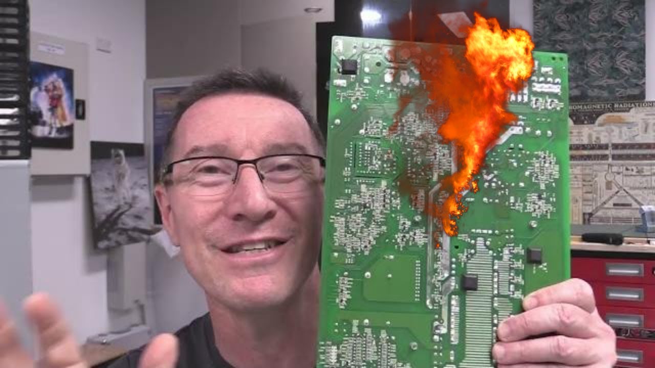
EEVblog 1559 - PCB Design: Trace Current Rating

preview_player
Показать описание
Dave answers a Twitter question: How should I design a PCB trace to carry 80A of current, and can this be done on one PCB layer? The answer is, well, complicated. Let's go down the PCB design rabbit hole of current rating PCB traces.

00:00 - Twitter question: How should I design a PCB trace to carry 80A of current
01:09 - Ohms law and copper losses
02:06 - PCB Trace calculator
02:45 - The three (four) major factors to PCB current handling calculations
02:54 - Trace Width and Copper thickness (weight) and PCB stackups
04:18 - A trap with Multilayer PCB designs
05:20 - External vs Internal layer matters with thermal design
06:20 - What happens if you exceed the maximum current rating?
07:23 - PCB plating matters
08:12 - Electrical vs Thermal design considerations
09:30 - 1oz copper vs 2oz vs 4oz
10:35 - Solder and tin plated traces
11:37 - Let's look at what a PCB manufacturer offers, HASL, SMOBC, ENIG etc
12:46 - How do you get your PCB traces plated in your design?
14:31 - Those are rookie temperature numbers, you gotta pump those up!
14:51 - The IPC 2152 and IPC 2221 standards are a bit How'ya'Doing
16:30 - The physical and thermal part of your product design matters
16:47 - Thermal conduction to planes matters
19:30 - Does VIA stiching matter?
20:30 - Have you considered a Bus Bar?
21:56 - We can get 80A on a single PCB trace, BUT...
23:18 - Can I interest you in bodge wire Sir? It's complete legit.
24:17 - PCB Standard WARS!
26:19 - Forget about etch factor
27:08 - Internal vs External trace calculations

Or with crypto:
BTC: 33BsprBQNBtHuVzVwDmqWkpDjYnCouwASM
ETH: 0x68114e40ff4dcdd384750500501e20acf3875f8c
BCH: 35n9KBPw9T7M3NGzpS3t4nUYEf9HbRmkm4
USDC: 0x68114e40ff4dcdd384750500501e20acf3875f8c
LTC: MJfK57ujxy55su4XicVGQc9wcEJf6mAoXF

Other channels:

#ElectronicsCreators #PCB #Design
Рекомендации по теме
Комментарии
Автор

Old PCB houses used to do roller tinned before solder mask, which gave you the crinkly soldermask, and of course if you wave soldered it then all the mask over wide traces would wrinkle and peel off, as the underlaying solder melted.

Also with a single 4oz layer on the board you will run into issues with warping, especially if you have a large board with a double sided load, you will have issues with components on the other side getting mechanical stress applied, so that you will have things like ceramic capacitors cracking and getting whiskers growing in them, and things like a BGA breaking loose from the balls, and other large SMD devices also suffering from either trace lifting, or joins cracking. Best solution is to take the big current and split it out to a separate board with all the high current paths on it, and then put a board interconnect to another board, which has all the control electronics on it. Bonus is then that any upgrade is easier, only half the board to redo, and also you go into a 3D volume, so the design overall will be smaller, as now your high current side is on a smaller board, which, even if it is a lot more expensive to buy, you get a lot more boards out of a single panel from the PCB house. Daughter board is a standard cheap 4 layer board from them, as a 4 layer board is almost default, if you do not want 4 layers, they simply etch all the copper away on the inner layers in the stack, and assemble them along with the other 4 layer boards. A bonus for the PCB house in the extra copper they get in the etchant recycling, extra profit.

SeanBZA
Автор

These days we have CPUs, GPUs and FPGAs dissipating 200-400 W, and pulling all that power in at 0.9-1.2 volts! The PCB currents and current densities must be insane, especially since you have to route all of this into multi-thousand pin BGA packages or LGA sockets, which also have hundreds of multi-GHz differential pairs snaking in and out, maybe even a 864 bit wide DRAM bus.

TheBackyardChemist
Автор

Current through a 1" wide trace will have crazy high current densities approaching even a large .093" circular pin. The transition from the THT pin to the 1" copper trace is most likely a larger problem than with the connector pin. A SMT high current FET will at least have a large surface are connection to the PCB trace unlike a THT part.

Solder has .1x the electrical conductivity of copper making it mostly impractical to get high currents using solder added on top of the trace. If the solder is 10x as thick as the copper you might get hale the resistance if you can keep the thickness consistent and controlled. There are also thermal conductivity issues and black body emmisivity issues with solder vs. copper and also important if you are pushing the limits.

Thank you for the introduction to Saturn PCB. It is a large step from my OLD Bishop Graphics PCB Design Handbook from the pre-CAD early 80's

Peter-House-Jr
Автор

It's also worth mentioning at 70 - 80 A you're at the practical limit of most TO style packages. Those bond 'wires' do pop if you push them too hard for too long and that seemly super low 0.004 ohm RDSon banner spec for your affordable MOSFET turns out to be 25 W! And that's before you realize that's the *typical*, your max RDSon spec is 0.007 ohms and with your CMOS or TTL level VGS drive means you're trying to dissipate 50W!

Also you have to think about protecting it as well, if it's an external connector you need to start worrying about adding ESD protection and other protections from uninformed users with their 48 V center negative PSUs they just love plugging into everything.

I've also seen a couple ultra high power density PCBs have thermal pads and heatsinking on the actual PCB traces which is always funny, I think the most recent example I saw it in was for some traces going to a 12VHPWR connector which does 50 A @ 12 V.

WizardTim
Автор

I really like this kind of content because it mixes theory and experience in a way that is directly applicable to solving engineering problems.

joelsciamma
Автор

Bus bars are really helpful, as they also serve as heatsinks. 1W per 1 square inch, passively cooled. 4W if actively cooled. 0.5mm copper sheets seem to be a good medium ground, and you can place several air-separated layers as fins. Soldering those bars is a bit of a hassle: you have to effectively heat-up the entire bar to ~200C, so use the largest soldering tip at your disposal.

squeaky_honda
Автор

dont forget that the high current also needs a return path

kubeek
Автор

Two simple answers and solutions: 1) lay one or more pieces of 12 AWG (2-3mm D) bare solid copper wire on the solder / tin plated trace (bend to follow the trace) and solder it to the trace. Most Plasma Cutter and Welder PCBs are made this way. No CAD, no tooling and almost no cost! Though you will need a high powered soldering iron with a large tip to solder the wire to the PCB.
2) get the largest (>1/4") solder wick braid and solder it to the HASL trace. Not quite as good as 12 AWG solid wire, but you can add more layers if needed. 🙂

shazam
Автор

More than food for thought "my old friend"... I don't comment a lot, but I just wanted to say thank you for all the knowledge and inspiration you brought to my own designs all over the years. After..., I would say a decade...or two...I still get Eureka moments from your videos that make me push a bit further....Thank you for your global public service :)

joaom
Автор

I had a board that distributed 30 - 40 Amps. I started with a .5" trace, added a slew of surface mount pads .5" x .5". The board arrived with what looked like a .5" solder tinned trace. I added some bare copper house wiring in #12 AWG and soldered it onto the trace using solder the whole way to add to the conductor area. Maybe I should have gone with #10 AWG. Anyway it was only about 8" or so. I had no issues.

jwb
Автор

Robert Feranec did some absolutely excellent videos on this subject btw!

p_mouse
Автор

Ken Wood (Saturn PCB), who wrote the calculator, does excellent work very quickly! I have used him for several PCB layouts.

Chris_Grossman
Автор

Part of the problem with switching 70-80 amperes with a MOSFET is the mosfet leads. The leads of a TO-220 melt at about 75 amperes and you also have to take into account the trace width available where the copper meets the device. Additionally just because a MOSFET die is rated for 100 amperes or more does not mean a real MOSFET is going to reliability handle that much current. Generally I would not push a PCB mounted MOSFET past 40 amperes and generally shoot for around only 20 amperes if surge currents are likely. Splitting the current between 2 or more devices allows the transistors to run at lower temperatures and gets the current paths down to a reasonable level.

briannebeker
Автор

It amazes me, that such a wise and experienced, by now old person whom I respect from the early days of the first episodes says: 12 inches - that's what she said.

You are just amazing. Genius!

HeartOfGermany
Автор

A 10 degC temp rise is really really small. Most PCBS are going to be sat in an ambient environment below 85 degC, so ime, depending on the duty cycle / duration of that high current you can carry far far higher than 20a on a 25mm trace!

One interesting experiment is to try to actually BLOW a trace. Find an old pcb, rig up a grunty power supply and try to blow some traces. You'll be surprised how much current and for how long you have to apply that current to cause the trace to delam, lift then fail. This is because the pcb has some thermal inertia. Heat produced does not immediately lead to a proportiojnally direct temperature rise because that heat is sunk away into the pcb.

This is why using an IMS (Interal Metal Substrate) pcb really really works well, and could be a very good solution to this problem. The trace generates heat, but that heat is sunk into the metal internal layer of the pcb. Add a suitable method of extracting that heat (passive or active heat sink) and you can run HUGE currents on small(ish) traces. I have a 3 phase IMS inverter board that runs up to 1, 000 amps and the entire inverter fits in a 100mm square area!!

maxtorque
Автор

Something that worked well for me once was square cross section bare copper for jewelry making. It was too springy out of the box so I threw it in the fireplace for a couple of minutes and then let it air cool. Clean it up with steel wool, and then bend it to fit over the PCB trace pretty well. Once one end is tacked down with solder flat on the trace and to the component pin you can tweak the fit as you go. I think I used 3mm copper, a little thinner than the trace. It is fine for DIY one-offs.

Solid core wire works but imo is harder to work with and get a neat job.

I never tried it but I guess if really desperate copper capillary tube might be good for water cooled traces.

karlharvymarx
Автор

Lol i felt the flex when you showed that big bus bar :), such great info as usual! ✨✨✨

Denyzyne
Автор

I was involved in the production of a new product that could run on line power or internal gelled lead acid batteries and that had a built in charger for the batteries. The circuit trace for routing charging power to the battery pack was protected by a 40 A fast blowing fuse. The trace itself was of 4 ounce copper and a single sided board. The trace ran along the edge, then turned a corner at the next edge of the board. There was a mounting screw near the corner so the trace tapered down then expanded back where it turned that corner. Barely over a quarter inch wide at the narrowest. Pretty loud pop when it blew up. Fuse was, of course, intact. For a temporary fix we soldered heavy copper braid on top of the trace of all the charging boards.

mikebarushok
Автор

You did not discuss how the current was going to flow in to or out of a pin from the MOSFET device into the trace and out to the final load. A 0.062" pad hole also will strain to accept or deliver that much current. Also it would have been nice to have seen a silver plating result vs solder plated result. .. Thanks for this practical application example video.

johnrussell
Автор

In my experience in most high current PCB cases you just have to accept +50°C above ambient, thick copper, and the fact that it should probably be a separate board with limited circuitry and size to prevent warping and even then you will need some extra tricks to really push it to the limit.

The reason for that is that if you even want such a current on a PCB it alredy means that it will most likely need to be a part of some circuit that will control the current (why even have that on a PCB otherwise). And since the circuit will probably require at least some protection you will have to roughly measure the current and since any shunts of such caliber are either huge and not PCB friendly or stupidly expensive or both you will want to use your trace as a shunt resistor. But with the decision now you actually need to have at least a few tens of millivolts of voltage drop across your trace as with high currents generally comes high noise of all kinds and it automatically puts you into a contradiction when you end up actually requiring to dissipate the power in your trace for the circuit to even work as intended. I have managed to push the compromise to 40A in one of my devices but I had the side of the single side populated board where the trace was covered by a thermal conductive sheet and screwed to a radiator or otherwise the whole thing would just get too hot.

Basically it can be done but it may not be quite as easy as one might expect. It is all a huge compromise and depending on the parameters required you may end up with no suitable solutions available at all.

Kirillissimus
welcome to shbcf.ru