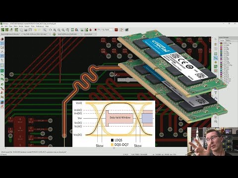
EEVblog #1247 - DDR Memory PCB Propagation Delay & Layout

preview_player
Показать описание
When does PCB propagation delay matter in PCB layout?
Dave goes down the rabbit hole from DIY TTL processor design to DDR memory design and layout.
DDR memory termination.
What is a timing budget? When is it important?
How does signal integrity matter?
When do you have to do serpentine PCB traces to match trace and differential pair lengths?

Micron DDR memory timing budget design:

#PCB #Layout #DDRmemory

Bitcoin Donations: 38y7DE8HEHNj8fGDtUr4PkCn9nWxiorvvy
Litecoin: ML7oQokTwB38bgzzjLDbRV97HKAHuwRfHA
Ethereum: 0x11AceA38DCA9DbFfB4F35f3F746af65F9dED28ce

Support the EEVblog through Patreon!

Buy anything through that link and Dave gets a commission at no cost to you.

Stuff I recommend:

Donate With Bitcoin & Other Crypto Currencies!

Рекомендации по теме
Комментарии
Автор

Another good tip for routing high speed signals is keep each trace on one layer from start to end; don't let it jump between layers, as you normally would do for low speed signals. Here is why. Suppose you are routing a signal with microstrip (that means the signal trace is on an outer layer, and the layer just beneath it is it's reference plane, usually ground). The current in the trace will return on the reference plane just beneath the trace. If you could see the return current in the plane, it would look like the shadow of the trace. Now suppose you jump the signal to an inner routing layer that is between two planes; this is now stripline, and it has two reference planes (usually one is ground and the other will be a power plane). So how does the return current follow the trace? If all the planes are the same potential (e.g. all grounds) then the return current will find it's way through the nearest via that connects the planes together. But if the plane vias are far from the trace via, you get a big loop, which looks inductive, and will cause a nasty reflection. So, if you absolutely must have your trace change reference planes (which is very common if it goes through a connector) make sure there are plane vias very close to the signal via. And if you are changing reference planes (from say, ground to 3.3V) then you must put a decoupling cap very close to the signal via, that couples the reference planes together.

steverobbins
Автор

As a software engineer with no formal hardware training, this very topic nearly caused me to quit doing electronics as a hobby. But then I did what you suggested and tossed out all the garbage I found online and started with some basic rules of thumb. I was over the moon when I printed my first USB3 hub board and it worked! Since then I have laid out some single-board Linux boards with ARM chips that use DDR memory and have had great success. My first couple of attempts failed, but then I took the courses on the FedEvel website and my next attempt was a success. There's a lot to learn on this topic, but if you just use some common sense and some good rules of thumb, and use your layout tools to your advantage, you can lay these PCBs out in no time.

testep
Автор

Yes! I want an in-depth guide to timing. It's frustrating me right now

entritur
Автор

At 35:40 - A common mistake, to match a differential pair with a squiggle 'somewhere' in one of the two signals. THAT SHOULD NEVER BE JUST SOMEWHERE IN THE MIDDLE. The pair is meant to be fully differential, and creating a length jump this way is like a phase jump. This means that at least on one side of the squiggle the pair is not balanced. The skew correction in a pair MUST be near the cause of the skew, e.g. the sideways leaving of a BGA pin pair.

ariedemuijnck
Автор

Another tip that I've picked up in the last year (still a young player mind you), is to take into account soldermask when routing on external layers. Rule of thumb I was taught for most soldermask is it'll reduce your Zo of the controlled impedance trace by roughly 1Ω per 1mil thickness of soldermask.

Another tip I've learned is if you do have to route DDR (or really any HS such as USB or QSPI SD), route your traces/lanes as perpendicular as possible to adjacent traces on adjacent layers (Shield with ground planes as much as possible). That way coupling will be reduced or nullified because right hand rule.

Last big piece is that it's not the frequency that matters, its the edge (rise/fall) rate of the signal that matters. If you slow down or slew/rate control your signal (while still meeting setup/hold times) you can minimize EMI and even help mitigate against reflections.

LorneChrones
Автор

I worked on a design last year with a FPGA and DDR3. Where I work we have people who do layout for us engineers. We were behind schedule so we thought we would kick the DDR3 to our layout guy before the schematic was complete so that he could get a start on what would be the most time intensive portion. In addition, we skirted some of the company process steps to rush into CAD, like constraining signals. Our layout guy came back to us a week or two later to review his work and it was immediately apparent that we shouldn't have trusted this guy to know how to route DDR lanes. Nowhere were there any serpentine traces. In fact, there was no attempt at all to length match traces. Each signal to the DDR took it's own path to get out of the chaos underneath the high density FPGA and the shortest trace was about 2 inches while the longest was about 10 inches. This was one of many mistakes on that project where cutting corners ended up costing more time to fix later.

sswpp
Автор

wow, I have to admit I don't understant much, but realizing how complicated PCB design can be is already a valuable lesson. Thank you for this one Dave!!

gl
Автор

Back in the day ... :-) I worked with an engineer that needed to delay an NMI signal to be slightly after the rising edge. He used what he called "Mickey Mouse Logic", placing 4 unused inverters in series between the source and target. It worked flawlessly at 1 Mhz. It was a bit eye opening for me at the time (I was like 19 or so), and has stuck with me ever since (this was in late 80's or early 90's).

russgibson
Автор

Trap for young players is to route busses on different layers.

Make sure to use exactly the same vias for each signal of a group. That way, manufacturing tolerances have no effect on your length matching. They all change together.

I just had to route a 16-bit DDR3L memory to an FPGA on a 20 x 20 mm PCB. That was NOT easy. Big boads are so much easier. Especially for length matching and crosstalk.

RandyLott
Автор

Amazing content! I am starting with SDRAM and this kind of crash-course video is invaluable. It is not only about the knowledge, but more importantly about understanding the whole scope of things we might not know, as well as the relative importance of them. Please continue.

OrbitalCookie
Автор

Propagation delay was an issue before many folks were born. The CDC 6600 used a backplane comprised of a mat of twisted pair wire ending in taper pins. Seymour Cray tweaked the lengths until things worked. One of my managers had the task of measuring the wires to which Seymour had attached a tag that said "TUNE", so that they could be used for the production machines. The clock for the 6600 was a blistering 10MHz.


Even before that, Grace Hopper used to pass out 1 ft. lengths of wire to her students, identifying them as "nanosecond" wires. (Light propagates at about a foot per nsec).

tubastuff
Автор

video about how to read a timing diagrams is a great idea.

timurvotyakov
Автор

How on earth do PC motherboard manufacturers manage to turn around these hugely complex designs so quickly? Imagine all the layout time, testing of the DDR4, PCI, SATA, NVMe, USB3 etc. And then charge less than £100 for them. Amazing.

gusbert
Автор

I'd love something on timing diagrams Dave!

zoeyk.
Автор

What I learned today: "You wouldn't want to go wigglety pigglety"

akuaku
Автор

And all this for Mhz-level signals, imagine the headaches designers have to go through for the current Ghz-level motherboards !

caiocc
Автор

I'd really like to see a video on those timing diagrams :)

theIpatix
Автор

Very informative Vblog, I hope you will have more in-depth videos about signal integrity and DDRs in future.

laad
Автор

A Video about signal integrity for high speed signals or differential pair impedance would be great!

danieltlang
Автор

Yes do a video on the timing diagrams. It took me forever to kind of understand what was going on with those and I would love to get a better understanding.

excitedbox