filmov
tv
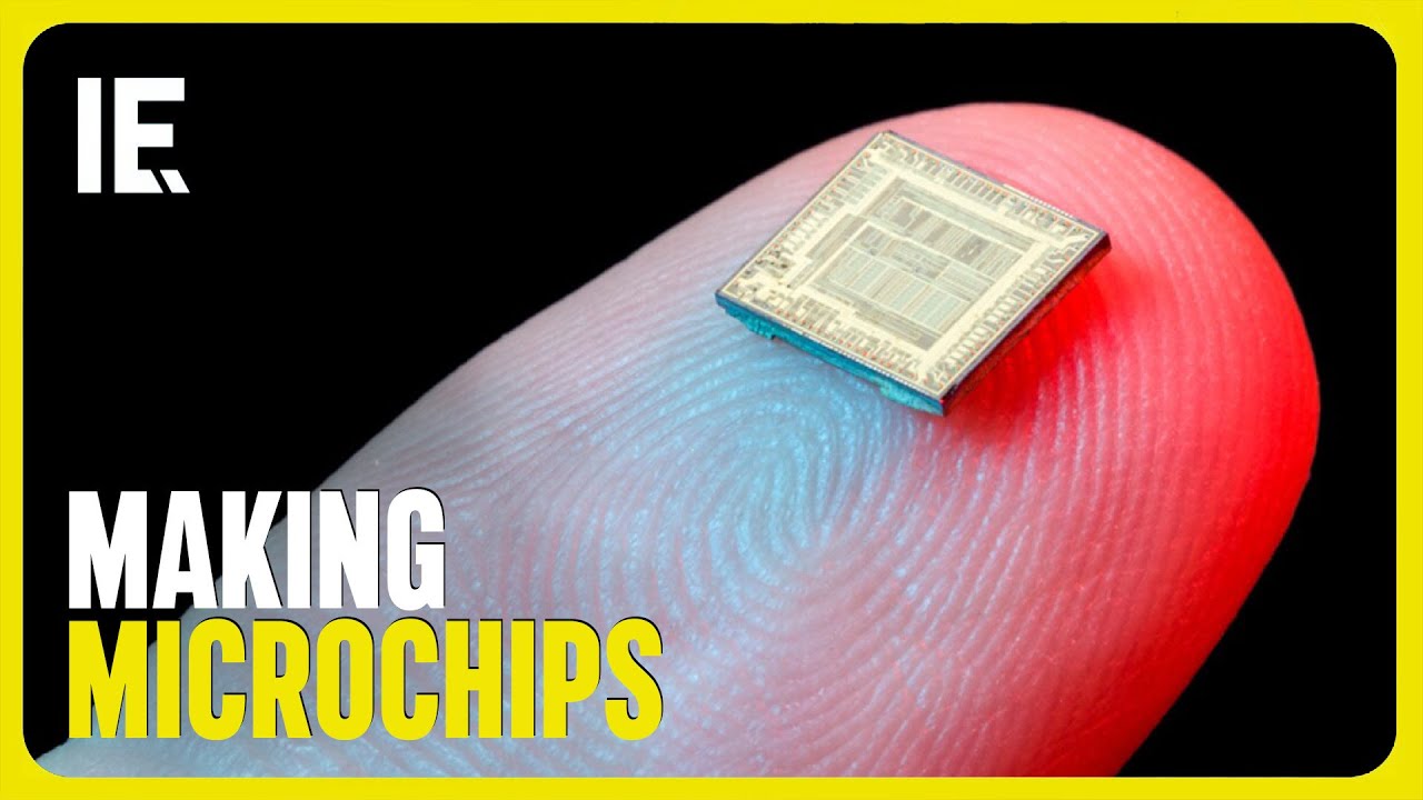
💻 How Are Microchips Made?
Показать описание
🤖 Want to know more about the latest tech and innovations? Don’t Miss Out!
——
💻 How Are Microchips Made?
Ever wondered how those tiny marvels powering our electronic world are made? From silicon-rich sand to intricate layers crammed with billions of transistors, the journey of a microchip is a fascinating tale of innovation and precision. Join us as we dive into the high-tech world of microchip manufacturing, where every step counts in creating the brains behind our devices. Stay tuned for a glimpse into one of our most complex feats of technology, where advancements are happening every day.
——
🎬 Main topics of the video:
📌 Microchip Production Process: Overview of how microchips are made, starting from the extraction of silicon from sand to the final testing and separation of individual chips.
📌 Silicon's Role: Silicon is highlighted as a crucial semiconductor material due to its ability to have its properties altered by adding impurities, making it suitable for various electronic devices.
📌 Manufacturing Steps: The process involves several critical steps such as deposition, lithography, exposure, doping, and etching, all performed in sterile conditions to avoid contamination.
📌 Component Composition: Microchips consist of capacitors, resistors, and transistors, with more advanced chips containing billions of transistors to enhance computational power.
📌 Moore's Law: The concept of Moore's Law, which predicts the doubling of transistor counts every two years, is mentioned as a driving force behind the continuous advancement in chip manufacturing technology.
📌 Technological Advancements: Despite the complexity of microchip manufacturing, continuous innovations have led to the production of more powerful chips with smaller transistor sizes, enabling enhanced performance in various electronic devices.
📌 Impact: Microchip manufacturing is portrayed as one of the most complex technological feats, with its advancements contributing significantly to the improvement of everyday devices like phones, computers, and gaming consoles.
——
🎥 Key Video Chapters:
0:00 - How long it takes to make a microchip
0:11 - How many transistors can be packed into a fingernail-sized area
0:26 - Why silicon is used to make microchips
1:15 - How ultrapure silicon is produced
1:39 - Typical diameter of silicon wafers
1:59 - Importance of sterile conditions in microchip production
2:18 - First step of the microchip production process (deposition)
2:43 - How the chip's blueprint is transferred to the wafer (lithography)
3:00 - How the electrical conductivity of chip parts is altered (doping)
3:35 - How individual chips are separated from the wafer (sawing)
3:47 - Basic components of a microchip
4:05 - Number of transistors on high-end graphics cards
4:54 - Size of the smallest transistors today
5:04 - SUBSCRIBE TODAY!
——
⚙️ About the Channel
At Interesting Engineering, our mission is to use storytelling to uncover the inner workings of the latest scientific breakthroughs, technological innovations, cultural phenomena, and more. We don’t just bring you breaking news. We uncover the mechanisms that make these developments possible, transforming how you see the world of today to ensure you’re prepared for the world of tomorrow.
#InterestingEgineering #Technology #Electronics #FutureTech #Gadgets #Innovation #Engineering #Artificialintelligence #IoT #AI #TechLife #CyberSecurity #Sustainability #ChipDesign
——
💻 How Are Microchips Made?
Ever wondered how those tiny marvels powering our electronic world are made? From silicon-rich sand to intricate layers crammed with billions of transistors, the journey of a microchip is a fascinating tale of innovation and precision. Join us as we dive into the high-tech world of microchip manufacturing, where every step counts in creating the brains behind our devices. Stay tuned for a glimpse into one of our most complex feats of technology, where advancements are happening every day.
——
🎬 Main topics of the video:
📌 Microchip Production Process: Overview of how microchips are made, starting from the extraction of silicon from sand to the final testing and separation of individual chips.
📌 Silicon's Role: Silicon is highlighted as a crucial semiconductor material due to its ability to have its properties altered by adding impurities, making it suitable for various electronic devices.
📌 Manufacturing Steps: The process involves several critical steps such as deposition, lithography, exposure, doping, and etching, all performed in sterile conditions to avoid contamination.
📌 Component Composition: Microchips consist of capacitors, resistors, and transistors, with more advanced chips containing billions of transistors to enhance computational power.
📌 Moore's Law: The concept of Moore's Law, which predicts the doubling of transistor counts every two years, is mentioned as a driving force behind the continuous advancement in chip manufacturing technology.
📌 Technological Advancements: Despite the complexity of microchip manufacturing, continuous innovations have led to the production of more powerful chips with smaller transistor sizes, enabling enhanced performance in various electronic devices.
📌 Impact: Microchip manufacturing is portrayed as one of the most complex technological feats, with its advancements contributing significantly to the improvement of everyday devices like phones, computers, and gaming consoles.
——
🎥 Key Video Chapters:
0:00 - How long it takes to make a microchip
0:11 - How many transistors can be packed into a fingernail-sized area
0:26 - Why silicon is used to make microchips
1:15 - How ultrapure silicon is produced
1:39 - Typical diameter of silicon wafers
1:59 - Importance of sterile conditions in microchip production
2:18 - First step of the microchip production process (deposition)
2:43 - How the chip's blueprint is transferred to the wafer (lithography)
3:00 - How the electrical conductivity of chip parts is altered (doping)
3:35 - How individual chips are separated from the wafer (sawing)
3:47 - Basic components of a microchip
4:05 - Number of transistors on high-end graphics cards
4:54 - Size of the smallest transistors today
5:04 - SUBSCRIBE TODAY!
——
⚙️ About the Channel
At Interesting Engineering, our mission is to use storytelling to uncover the inner workings of the latest scientific breakthroughs, technological innovations, cultural phenomena, and more. We don’t just bring you breaking news. We uncover the mechanisms that make these developments possible, transforming how you see the world of today to ensure you’re prepared for the world of tomorrow.
#InterestingEgineering #Technology #Electronics #FutureTech #Gadgets #Innovation #Engineering #Artificialintelligence #IoT #AI #TechLife #CyberSecurity #Sustainability #ChipDesign
Комментарии
 0:27:48
 0:05:35
 0:08:59
 0:08:40
 0:01:40
 0:14:36
 0:23:01
 0:05:25
 0:06:35
 0:12:05
 0:03:25
 0:04:45
 0:02:42
 0:09:07
 0:07:44
 0:21:51
 0:18:40
 0:07:22
 0:02:41
 0:08:12
 0:56:39
 0:05:46
 0:10:31
 0:24:56