filmov
tv
How Microchips Are Made - Manufacturing of a Semiconductor
Показать описание
#chipmanufacturing
How are microchips made - from sand to semiconductor: Microelectronics usually is hidden to society – however, it is a constant companion in our daily lives. It tremendously contributes to the ongoing development and digitization of our world. But what is actually behind this technology?
Read more about microchip manufacturing and the importance of wafers or semiconductor chips here:
-----------------------------
 0:05:35
💻 How Are Microchips Made?
 0:27:48
How are Microchips Made? 🖥️🛠️ CPU Manufacturing Process Steps
 0:08:40
How are BILLIONS of MICROCHIPS made from SAND? | How are SILICON WAFERS made?
 0:08:59
HOW IT'S MADE: Microchips
 0:01:40
How To Make A CPU
 0:12:05
How Microchips Are Made
 0:14:36
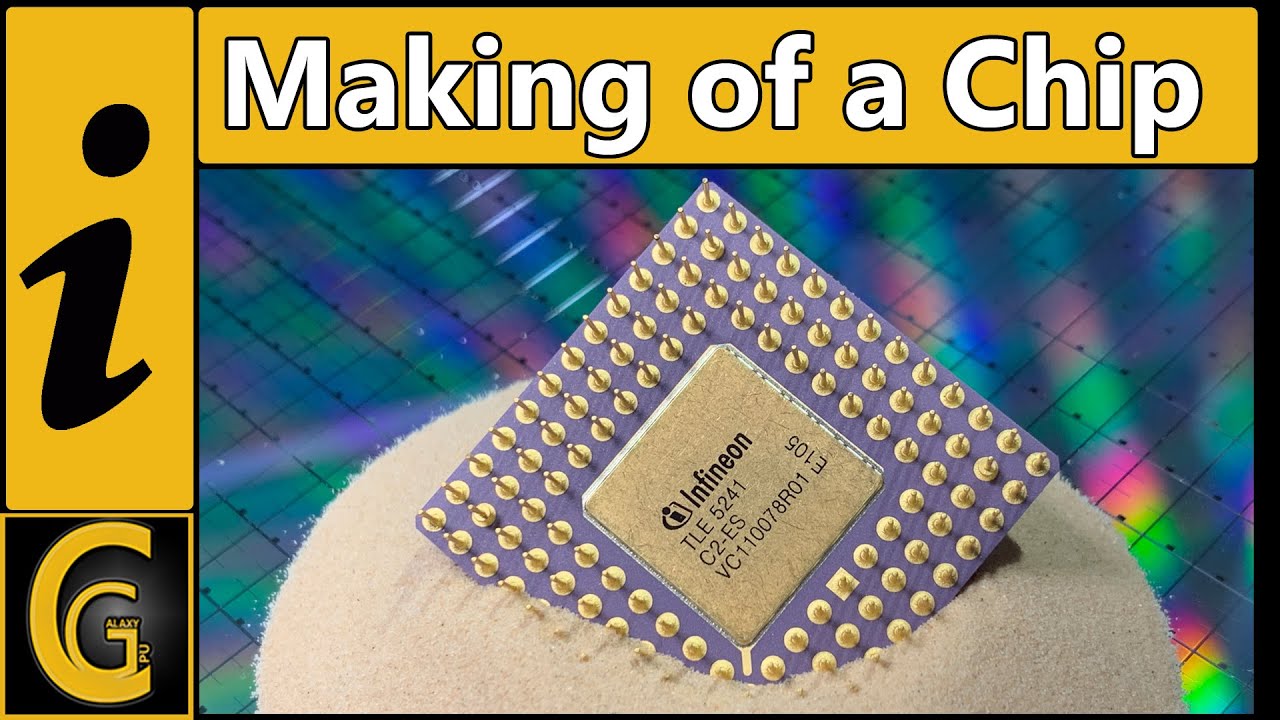
How Microchips Are Made - Manufacturing of a Semiconductor
 0:05:25
Uncovering the Silicon: Demystifying How Chips are Built and How They Work
 0:23:01
Inside Micron Taiwan’s Semiconductor Factory | Taiwan’s Mega Factories EP1
 0:06:35
The Entire World Relies on a Machine Made by ONE Company
 0:03:25
How Microchips are Made
 0:05:46
'Z2' - Upgraded Homemade Silicon Chips
 0:02:42
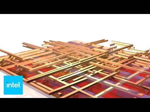
Intel: The Making of a Chip with 22nm/3D Transistors | Intel
 0:18:40
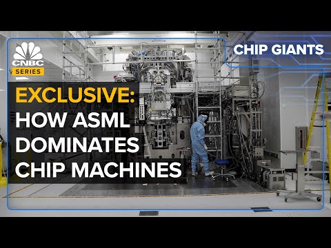
Why The World Relies On ASML For Machines That Print Chips
 0:08:12
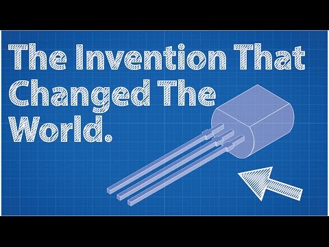
Transistors - The Invention That Changed The World
 0:07:44
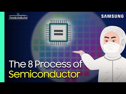
‘Semiconductor Manufacturing Process’ Explained | 'All About Semiconductor' by Samsung Sem...
 0:04:45
From Sand to Silicon: The Making of a Microchip | Intel
 0:07:22
How Are Microchips Made?
 0:03:44
History of Microchips
 0:06:56
How Microchips are Made in the Factory
 0:00:55
Super Advanced Micro-Chips Made By Ancient Indians!!
 0:01:01
How microchips are made?
 0:10:31
How CPUs are Made: From Sand to Wafers to Chips
 0:01:00
Process Of Making Silicon In a Factory
Комментарии