filmov
tv
HOW IT'S MADE: Microchips

Показать описание
HOW IT'S MADE Microchips
Microchips are everywhere! With the advent of amazing technology comes a greater need for efficient microchips. But they sound minuscule, so if you’re wondering about how they are made, we’ll discuss that in our video!
Welcome back to How It’s Made, folks, and today we’ll be talking all about microchips! But before we delve into the world of manufacturing, hit that subscribe button, if you haven’t already!
What is a microchip?
Microchips are a flat silicon disk that has an integrated circuit embedded on it and even incorporates transistors. There are patterns of tiny switches that are created on the silicon wafer by embedding materials to form a deep and integrated lattice of interconnected shapes. There are elaborate processes that lead to the construction of these interconnected circuits, and we’ll discuss all of them in detail.
Raw Material: Silicon
Silicon is the digital gold in the technology industry as it is a widely used semiconductor. The manufacturers often improve the properties of the semiconductor by adding phosphorus or boron. The great news is silicon is made from sand which is the second most popularly found element after oxygen.
Silica sand is a form of silicon dioxide from which silicon wafers are made. The first step for this is by melting the sand into a shape of a large cylinder called an ingot from where the thin wafers are sliced off.
For microchips, good and pure silicon is always a mandatory material hence, only one impurity atom, for every 10 million silicon atoms is allowed. Silicon bulls are made in a range of different diameters where the most common sizes are 150, 200, and 300 millimeters wafers! Now, for microchips, the silicon wafers must be really thin. Hence, there is a special sawing technique where these wafers are made.
Why is silicon used?
Silicon is a semiconductor that is an efficient conductor of electricity provided certain conditions are fulfilled. Every silicon atom has four outermost electrons because of which actual pure monocrystalline silicon is non-conductive at room temperature. To make it conductive, small quantities of specific atoms are to be added as impurities to the wafer.
This process is called doping and most often, boron and phosphorus atoms are highly used. The most suitable elements in these groups are very close to silicon on the periodic table and thus have very similar properties.
The P and N conductive layers are very important and the most important part of the chip is the transistors that are built on the P and N conductive layers. The wafer transistors are the smallest control units in microchips. Their job is to control electric voltages and currents.
They are by far the most important components of electronic circuits as every transistor on a chip contains P and N conductive layers. These layers are made of silicon crystals and they also have an additional layer of silicon oxide which acts as an insulator. A layer of electrically conductive polysilicon is coated on top of this.
How are microchips made?
Step #1. Layout and Design
Microchips have to always be carefully designed as these are highly complex chips that are made up of billions of integrated and connected transistors that make up complex circuits such as microcontrollers and crypto chips.
A few square millimeters have to be measured in size and carefully outlined. The actual number of microcomponents requires an in-depth design process that defines the chip’s functions. This actually characterizes the chips’ technical and physical properties.
In fact, special design tools are used to draw up the plans for integrated circuits and construct a three-dimensional architecture of sandwich layers. This blueprint is transferred to photomasks to give the geometric images of the circuits.
The photomasks are used as image templates during the subsequent chip fabrication process to make sure that the microscopic structures of a chip are reproduced perfectly. These are the patterns you’d be seeing on the microchip.
They have to be made in a dust-free environment with stable temperature and humidity levels.
Step #2. Putting it together in a cleanroom.
The chips have to be made in a cleanroom where no more than one particle of dust larger than 0.5 micrometers is allowed in around 10 liters of air. This place is extremely sophisticated with several million cubic meters of air being circulated every hour and hundreds of air volume regulators maintaining a constant airflow. The employees in these production areas have an extremely strict dress code.
It is here that all the airlock chips are built on a base wafer that is cut from a silicon ingot, depending on their size. Several dozen or several thousand chips can be made on one wafer because of their small size.
#Howitsmade #microchips #howitsdone
 0:08:59
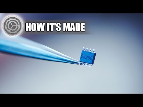
HOW IT'S MADE: Microchips
 0:05:35
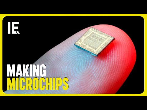
💻 How Are Microchips Made?
 0:27:48
How are Microchips Made? 🖥️🛠️ CPU Manufacturing Process Steps
 0:09:35
How It's Made: Microchips in Factories
 0:08:40
How are BILLIONS of MICROCHIPS made from SAND? | How are SILICON WAFERS made?
 0:14:36
How Microchips Are Made - Manufacturing of a Semiconductor
 0:12:05
How Microchips Are Made
 0:02:41
How are microchips made?
 0:06:11
How a CPU is Made / Microchips (Animation)
 0:07:22
How Are Microchips Made?
 0:03:25
How Microchips are Made
 0:01:01
How microchips are made?
 0:06:46
From Sand to Silicon: How are Microchips Made?
 0:05:28
How it's made Microchips ASML
 0:00:55
Super Advanced Micro-Chips Made By Ancient Indians!!
 0:09:04
Microchips: How It's Made
 0:06:56
How Microchips are Made
 0:11:48
How It's Made: Computer And Microchips
 0:04:17
World of Chips, Episode 6: How a Chip is Made -- Steps 1 - 3 | Synopsys
 0:00:21
how Microchip made from Silicon
 0:02:34
Inside a Microchip Factory : How Microchips are Made
 0:03:51
How are Microchips made I @ILabs365 I What are computer made of I Microchip I integrated circuit
 0:05:20
How is the Microchip made ? | Microchip manufacturing || sand - chip ? || making I.C ??
 0:12:38
How It’s Made : Inside a French Potato Chip Factory
Комментарии