filmov
tv
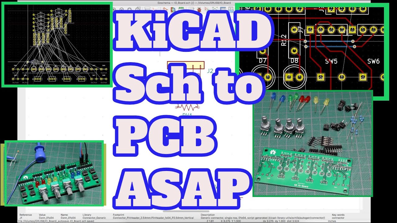
KiCAD Schematic and PCB - Quick Design Example and Build
Показать описание
In this KiCAD design example, we design a schematic based on a simple circuit, then the PCB layout, and upload gerber files for manufacturing. This goes very quickly and isn’t intended to cover everything, just a brute force Quickstart to get a feel for the tool. Other people’s tutorials may supplement this one if it’s not comprehensive enough!
When the boards arrive, we assemble and test them to be sure they perform the intended functions.
Schematic and KiCAD files:
 0:13:16
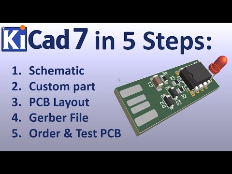
KiCAD 7 PCB Layout in 5 steps
 0:19:50
KiCAD Schematic and PCB - Quick Design Example and Build
 0:02:32
Get from Schematic to PCB Faster | KiCad 6.x Quick Tips
 0:00:50
KiCad 6: Update PCB Layout From Schematic
 0:00:59
Best and Worst PCB Design Software
 0:20:13
KiCad 6 tutorial - Start to finish board design
 0:22:46
How to design an ESP32 PCB with KiCad (in less than 25 minutes)
 0:14:41
How to make your First PCB! Beginner KiCAD Design Tutorial
 0:07:46
#3 How To Design A Circuit Using KiCad 7.0 Schematic Editor | #PCBCupid
 0:09:12
Build a KiCad Project Schematic | Part 1
 0:25:43
Convert a Schematic Drawing to PCB using KiCad : Reverse Engineering a 6502 CPU card
 0:11:05
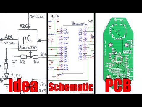
From Idea to Schematic to PCB - How to do it easily!
 0:06:10
Making schematics and PCBs with KiCad - part 1
 0:00:20
KiCAD | PCB Design & Development | 3D Model
 0:37:37
How To Make a PCB With No Experience! [KiCAD 8.0 Schematic Tutorial #1]
 1:40:06
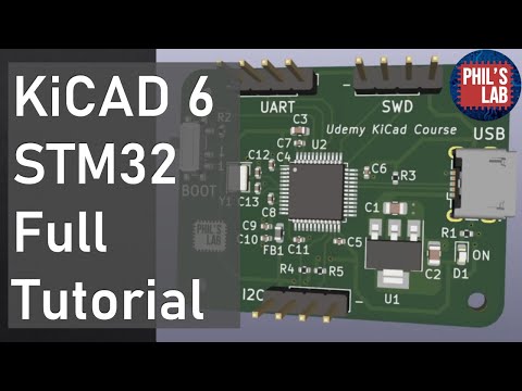
KiCad 6 STM32 PCB Design Full Tutorial - Phil's Lab #65
 0:12:16
Kicad schematics and PCB Python scripting
 0:00:33
My first #RaspberryPi #RP2040 board works! #microcontroller #electronics #DIY #circuits #kicad
 0:00:07
Secret To Design A PCB in KiCad 7
 0:18:09
Creating Simple Schematics with KiCad
 0:10:33
Learn Schematic and PCB Design [STM32] - Part 1 (KiCAD V.7)
 0:20:19
How to Design Mechanical Keyboard PCBs with Kicad
 0:00:41
kicad schematic to pcb #kicad #tutorial #schematics #pcb #layout #art
 0:16:35
#17 - KiCad - PCB layout replication
Комментарии