filmov
tv
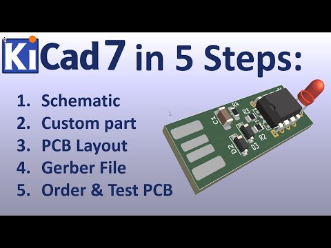
KiCAD 7 PCB Layout in 5 steps

Показать описание
In this video we will make a PCB from scratch with KiCAD 7.
I will use the DIY Digispark USB circuit from a previous video as an example.
and guide you through all the steps:
0:00 Introduction
0:44 Schematic drawing
2:55 Create a custom symbol
4:21 Create custom footprint
6:39 PCB Layout
8:20 Create multi-PCB panel
10:54 Generate Gerber & Drill files & order PCB
12:22 Build & test the circuit.
Links:
Note: To use a PCB as USB like this you need to have a total thickness of ~2.2 mm for proper contact. To achieve this you can glue 0.6mm thick material on the back (I cut it from a plastic lid ;-).
 0:13:16
KiCAD 7 PCB Layout in 5 steps
 2:01:32
Master New KiCad 7 In Under 2 Hours | #PCBCUPID
 0:05:50
Tame the yellow line: Master KiCad 7 Edge.Cuts
 0:09:49
#10 How To Do PCB Routing In KiCad 7.0 with Basic PCB Design Rules | #PCBCupid
 2:25:30
KiCad 7 ESP32 PCB Design Full Tutorial - made by morten laboratories iot-thing
 0:00:07
Secret To Design A PCB in KiCad 7
 0:07:58
#7 How To setup PCB STACKUP in KiCad 7.0 | #PCBCupid
 1:40:06
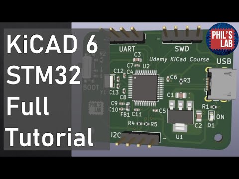
KiCad 6 STM32 PCB Design Full Tutorial - Phil's Lab #65
 0:19:50
KiCAD Schematic and PCB - Quick Design Example and Build
 2:07:51
KiCad 7 STM32 Bluetooth Hardware Design (1/2 Schematic) - Phil's Lab #127
 0:31:43
KiCad Design Tutorial (Teil 2): Platine (PCB) in 8 Schritten erstellen (deutsch)
 0:10:58
Boost Your PCB Design Productivity | 7 Best Plugins for KiCad
 0:05:40
Quickstart Intro to Kicad - Design a board in 5 minutes
 0:10:50
KiCAD 7 Autorouter – Simple Fast Prototyping
 0:07:46
#3 How To Design A Circuit Using KiCad 7.0 Schematic Editor | #PCBCupid
 0:04:50
#1 How To Use New Kicad 7.0 - Introduction | #PCBCupid
 2:56:53
KiCad 7 STM32 Bluetooth Hardware Design (2/2 PCB) - Phil's Lab #128
 0:22:46
How to design an ESP32 PCB with KiCad (in less than 25 minutes)
 0:00:08
Received PCB From Various Manufacturers - KiCad 7 tutorial series #pcb #electronics
 0:00:31
H Bridge PCB Layout in 30 seconds using Kicad
 0:12:18
Mastering KiCad: Design & Build Your Custom Stereo Amplifier Board!
 0:28:54
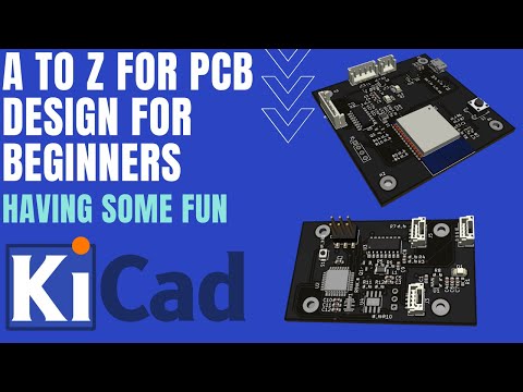
KiCad Tutorial - A to Z of PCB Design for Beginners
 0:01:00
Make PCB panels in kicad! #pcbcupid #electronics #kicad
 0:10:56
Basic KiCad 2-Layer PCB Routing Demonstration
Комментарии