filmov
tv
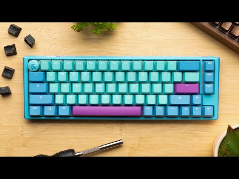
How to Design Mechanical Keyboard PCBs with Kicad

Показать описание
Today we're going to be taking a look at just how simple it is to design your own mechanical keyboard PCB within Kicad. We will cover everything from setting up the program along with applicable symbol and footprint libraries, designing the schematic, laying out the PCB, and finally some information on the differences between HASL and ENIG when ordering.
~ Links ~
~ Handwiring Tools ~
~ Handwiring Parts ~
~ 3D Printing ~
~ Favorite Cheap Switches ~
~ Social ~
~ Community ~
~ Timestamps ~
0:00 - Intro
0:22 - Setup
2:48 - Schematic
7:35 - Footprint Assignment
8:43 - PCB Setup
9:14 - Grid System
10:04 - Positioning
13:55 - Routing Traces
15:37 - Vias
16:17 - Controller Wiring
16:46 - Design Rules Checker
17:00 - Edge Cuts
17:38 - Filled Zones
18:45 - Exporting Gerbers
18:56 - Ordering PCBs
19:15 - HASL vs ENIG
19:58 - Outro
~ Disclaimer ~
Some links may be affiliate links where I will make a small commission. Nothing in this video was sponsored by any outside party and I wasn't paid for the content in this video.
#mechanicalkeyboard #kicad #pcb
 0:20:19
How to Design Mechanical Keyboard PCBs with Kicad
 0:25:08
Build your own Mechanical Keyboard… the RIGHT Way
 0:11:16
How to Design Mechanical Keyboard Plates and Cases
 0:08:01
How to Build a Custom Keyboard From Scratch | Part 1 Layout and Design
 0:00:18
Wood Keyboard Surprise 😲🪓
 0:11:51
Beginner's Guide To Mechanical Keyboards
 0:16:12
How to Build a Mechanical Keyboard | Simple Step-by-Step Guide | MODE Sonnet
 0:23:56
How to Design a Custom Mechanical Keyboard
 0:02:16
Budget Hall Effect Keyboards Just Got Better...
 0:22:13
How I Turned my Idea Into a Product – The Encore Keyboard
 0:00:15
One Piece Keycaps #shorts
 0:16:20
If Apple Made Custom Mechanical Keyboards - The MODE Experience
 0:41:51
Designing and Building a Mechanical Keyboard
 0:48:38
PART 1: Designing a custom mechanical keyboard from scratch | #KiCAD | #mechanicalkeyboard
 0:00:34
The COOLEST Keycap EVER?!
 0:20:30
“The REAL Ergonomic Keyboard Endgame!” - How To Design & Make A Totally Custom Keyboard
 0:00:27
How is this keyboard SO GOOD!? 😱
 0:00:19
The ULTIMATE Upgrade for Your Gaming Keyboard!?!?
 0:00:17
Satechi SM1 Slim: The Stylish Mechanical Keyboard for Mac & Windows
 0:10:22
Bringing a Product to Market – How I Designed Custom Keycaps
 0:14:25
DIY Macro Pad Keyboard Build from Scratch with Custom PCB and Mechanical Switches
 0:00:29
Building a Drop Alt Custom Keyboard Part One ⌨️
 0:00:12
Budget creamy keyboard with nice design, Aula F65 #tech #setup #keyboard #asmr
 0:00:37
An Actually Good Gaming Keyboard With a Cool Design
Комментарии