filmov
tv
An Intro to KiCad – Part 2: Create a Schematic Symbol | DigiKey

Показать описание
In Part two Shawn provides a detailed walkthrough of creating a custom schematic symbol in KiCad V4.07. Using a datasheet for a 7555 timer as a reference, Shawn creates Pins, assigns Pin labels, and lays them out according to his project. Not every part requires custom symbol creation and by utilizing Digi-Key’s symbol and footprint library you can create your schematic and layout your board much faster.
Learn more about:
Learn more about:
 0:05:40
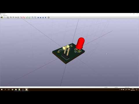
Quickstart Intro to Kicad - Design a board in 5 minutes
 0:11:10
An Intro to KiCad – Part 1: How PCBs Are Made | DigiKey
 0:15:50
An Intro to KiCad – Part 3: Schematic Capture | DigiKey
 0:13:16
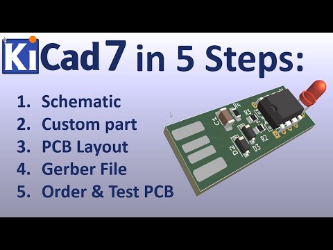
KiCAD 7 PCB Layout in 5 steps
 0:11:18
An Intro to KiCad – Part 2: Create a Schematic Symbol | DigiKey
 0:18:15
An Intro to KiCad – Part 7: Board Layout | DigiKey
 0:16:54
An Intro to KiCad – Part 6: Place Parts and Define Outline | DigiKey
 0:14:04
An Intro to KiCad – Part 9: Generate BOM and Order Parts | DigiKey
 0:20:16
An Intro to KiCad – Part 4: Create a Footprint | DigiKey
 0:09:09
An Intro to KiCad – Part 8: Generate Gerbers and Order Boards | DigiKey
 0:15:37
An Intro to KiCad – Part 5: Associate Footprints and Generate Netlist | DigiKey
 0:04:50
#1 How To Use New Kicad 7.0 - Introduction | #PCBCupid
 2:39:53
Introduction To KiCAD
 0:20:24
KiCAD Quick-Start Tutorial
 0:07:43
An Intro to KiCad – Part 10: Solder Components to the PCB | DigiKey
 0:53:52
Introduction to KiCad 6.0 OR Getting Started in KiCad 6.0
 0:29:24
Kicad introduction
 0:23:48
KiCAD Tutorial 2019 | Learn KiCAD under 25 Minutes | Beginners guide
 0:20:28
How To Design A PCB on KiCad from Start to Finish (Easy Guide)
 0:18:32
Introduction to KiCAD - Part 0
 0:43:24
Introduction to KiCAD - Part 1, Schematics
 0:44:57
Learn KiCad 8 in 45 minutes - From idea to upload in one video
 0:00:08
Received PCB From Various Manufacturers - KiCad 7 tutorial series #pcb #electronics
 0:00:48
KiCad - Zero to Hero 1 | Introduction: What we'll make
Комментарии