filmov
tv
Analog Chip Design is an Art. Can AI Help?

Показать описание
Notes:
I say that digital design is roughly the same size. Sometimes they have to be different sizes for the purpose of optimizing of delay/speed - usually by a factor of 3 or 4. That has some interesting consequences in FinFET design but we can talk about that someday later.
Links:
I say that digital design is roughly the same size. Sometimes they have to be different sizes for the purpose of optimizing of delay/speed - usually by a factor of 3 or 4. That has some interesting consequences in FinFET design but we can talk about that someday later.
Links:
 0:15:48
Analog Chip Design is an Art. Can AI Help?
 0:01:22
A Day in the life of an Analog IC Engineer
 0:12:11
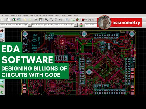
Designing Billions of Circuits with Code
 0:16:25
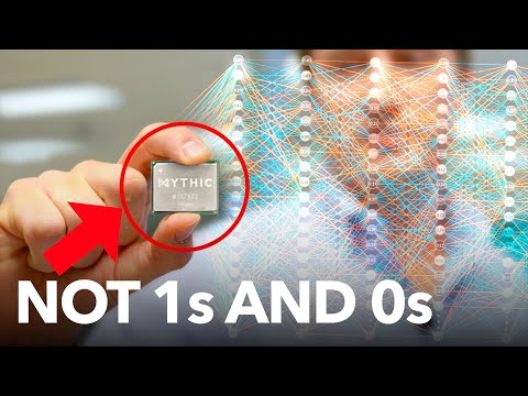
Memristors for Analog AI Chips
 0:21:42
Future Computers Will Be Radically Different (Analog Computing)
 0:11:51
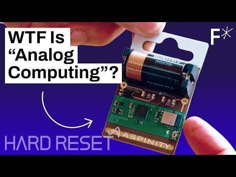
Analog computing will take over 30 billion devices by 2040. Wtf does that mean? | Hard Reset
 0:09:58
HWN - '20-year Analog IC Designer' vs Our Team (Interview Question)
 0:17:36
Why the Future of AI & Computers Will Be Analog
 0:23:12
The Ultimate DAC- Playback Designs!
 0:15:28
Analog Computing is GENIUS - Here's Why!
 0:01:49
Analog IC Design - Introduction Video
 0:05:08
These Chips Are Better Than CPUs (ASICs and FPGAs)
 0:01:31
New Analog Chip Design #science #news #computer
 0:00:24
Does Analog design have a future? What about AI? 🤔🤔 #vlsi #chipdesign
 0:02:56
Common Analog, Digital, and Mixed-Signal Integrated Circuits (ICs)
 0:40:11
Open Source Analog ASIC design: Entire Process
 0:00:59
Day 11/75 Engineering Things | Analog Chip Design Vs Digital Chip Design
 0:13:18
Google’s Chip Designing AI
 0:01:55
The world's largest analog chip designer
 0:09:30
HWN - Analog Design Interview Question
 0:00:30
5 Channels for Analog VLSI Placements #texasinstruments #analogelectronics #analog #nxp
 0:05:35
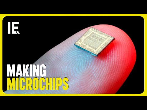
💻 How Are Microchips Made?
 0:04:54
Why are we moving to digital? - Analog vs. Digital in 5 minutes | Digital Hardware Design #1
 0:13:00
Analog Simplified
Комментарии