filmov
tv
PCB Design Tutorial Start to Finish

Показать описание
Here are some shortcuts I used throughout the video:
[ - rotate left
] - rotate right
f - change tracing elbow (SCH and PCB)
w - cycle through preferred trace widths (PCB)
Also for those who are curious, at 03:20, when I imported other rules, I did so by selecting the ruleset and copy pasting it across a different flux instance: CTRL+C,CTRL+V.
00:00 - Intro
00:32 - New Project
00:41 - Description, Permissions
01:03 - Comments
01:26 - Library
01:37 - Generic Components
01:54 - Part Properties
01:59 - Alignment in SCH
02:13 - Tracing in SCH
02:39 - Portals
02:54 - Board Shape in PCB
03:20 - Remove Silk with Rules
04:03 - Layout Tips
04:17 - Alignment in PCB
04:42 - Tracing in PCB
04:53 - Preferred Trace Widths
05:55 - Vias
06:30 - Silk Logo
07:18 - Silk Text
08:07 - Copper Fill
08:24 - Adding Part Properties for BoM
09:23 - Manufacturing Export
09:40 - PCBWay Order
 0:10:40
PCB Creation for Beginners - Start to finish tutorial in 10 minutes
 0:10:21
PCB Design Tutorial Start to Finish
 0:18:49
How To Learn PCB Design (My Thoughts, Journey, and Resources) - Phil's Lab #87
 0:16:30
Learn PCB Designing in 15 Minutes
 0:11:05
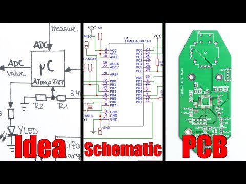
From Idea to Schematic to PCB - How to do it easily!
 0:10:44
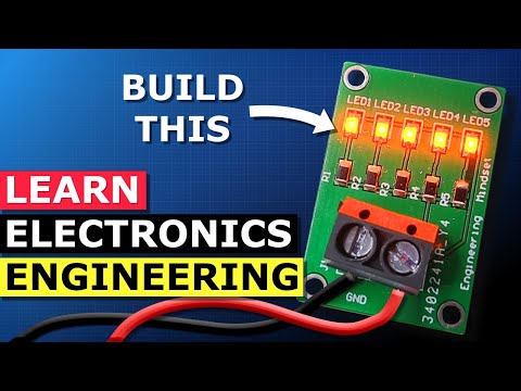
Design and Build a PCB - SMD LED Learn electronics engineering
 0:23:37
Altium Designer Quick-Start Tutorial with Phil Salmony from Phil's Lab
 0:09:28
How To Make Custom PCB's For Your Projects!
 0:45:07
Dielectric Anisotropy Implications for Transmission Line Impedance & Via Modeling | Sierra Circu...
 0:12:43
Dive into PCB Design: Kicad 8 Tutorial for Beginners
 0:00:59
Best and Worst PCB Design Software
 0:13:16
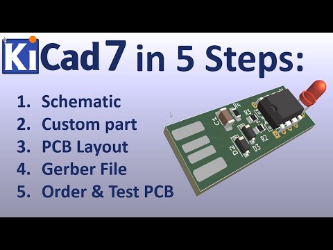
KiCAD 7 PCB Layout in 5 steps
 2:20:05
Designing a PCB LIVE - Start to Finish + Tips
 0:05:29
Fusion How-To: Design Your First PCB Schematic | Autodesk Fusion 360
 1:40:06
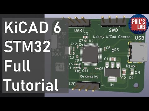
KiCad 6 STM32 PCB Design Full Tutorial - Phil's Lab #65
 0:33:32
From Zero to PCB | using Altium Designer
 0:08:42
PCB Design - Getting Started & Design Rules
 0:05:51
PCB Design For Beginners: Ugly Tracks Are Noisy
 0:16:43
EasyEDA Full TUTORIAL + Create Component + TIPS
 0:25:54
Introduction to Basic Concepts in PCB Design
 0:13:45
🔥Roadmap to Start Learning PCB Design from Scratch | How to Design PCB ?
 9:02:56
Complete PCB Design Course in OrCAD and Allegro 17.4 | OrCAD & Allegro PCB Design by LtlBiTech
 0:12:52
Top 5 Beginner PCB Design Mistakes (and how to fix them)
 0:33:10
An Absolute Beginners Guide To Designing PCBs using Easy EDA - Make PCB From A Schematic
Комментарии