filmov
tv
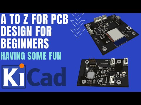
KiCad Tutorial - A to Z of PCB Design for Beginners

Показать описание
#KiCad #PCB #Beginners
KiCad Tutorial - A to Z of PCB Design for Beginners
00:00 Intro
00:44 A - Add or Append
01:16 B - Board Outline
02:57 C - Copper Tacks or Copper Pour
05:40 D - Design Rules
06:30 E - Edit
07:57 F -Fiducial
08:35 G - Gerbers
09:40 H - Holes
10:47 I - Images
11:33 J - Just do it
12:01 K - Keep out
13:05 L - Layers
14:17 M - Mechanical
15:28 N - New Project
16:19 O - Overlay
16:38 P - Place Component
18:09 Q - Questions
18:50 R - Rats Nests
19:30 S - Soldermask
20:22 T - Text
22:11 U - Unconnected Tracks
23:11 V - Vias
24:30 W - Wire
25:21 X - X outs
26:23 Y - Why?
26:54 Z - Zero Position
28:04 Outro
In this video, we have a little fun with the alphabet. Explaining KiCad PCB Design from A to Z. This video is aimed at beginners and people who are new to PCB design. At the top, you can press on what letter of the alphabet you would like to focus on :)
This is supposed to just highlight some terms and principle, I do not go into to much detail otherwise we will be here the whole day :)
Will make independent videos on each letter.
Let me know your why?!?!
If you feel like this video helped, please leave a comment below and let us know if there are any other PCB tutorials you would like.
Below you can find all other useful links that might help you.
📚Altium Tutorials📚
📚KiCadTutorials📚
📚Let's learn circuit Playlist📚
💻All our PCB Design - Github💻
💻Download your free Altium Designer 20 for 6 months💻
-----
Have a great week and stay safe :)
Комментарии
 0:13:16
 0:22:46
 0:22:16
 0:44:57
 0:09:48
 1:40:06
 0:05:40
 2:25:30
 0:04:56
 0:28:54
 0:14:41
 0:09:57
 0:23:48
 0:20:19
 0:24:18
 2:01:32
 0:11:59
 0:12:43
 0:22:46
 0:06:57
 2:07:51
 0:32:27
 0:00:16
 0:31:43