filmov
tv
Master New KiCad 7 In Under 2 Hours | #PCBCUPID

Показать описание
This video is a 2hr compilation of our KiCad Series, which walks through the complete process of PCB development from scratch, while discussing all the important part of PCB Design :
• Learning basic tools and navigation
• Building Schematics
• Performing Electrical Rule Check
• Assigning Footprints
• Understanding PCB Stackup / Netclasses
• PCB Layout
• Routing
• Performing Design Rule Check
• Creating Custom Symbols and Footprint
• PCB Optimization for Production
If you like to learn what is PCB You can check out our website PCB CUPID:
Make sure to subscribe and share this content with someone who would love this!
▬▬▬▬▬▬ Follow us on other social media platforms! ▬▬▬▬▬▬
▬▬▬▬▬▬ Contents of this video ▬▬▬▬▬▬
0:00 - intro
0:15 - Introduction to KiCAD
4:13 - KiCAD UserInterface
9:48- Schematic
16:45- Prettify Schematic
22:00- Electrical Rules Check
26:22- Footprint Assignment
38:42- Understanding PCB Stackup
46:05 - Predefined Rules & Constraints
56:58- PCB Layout
01:04:42 - Routing
01:13:30- Design Rule Check
01:23:42 - Gerber File Generation
01:31:00 - Custom Symbol
01:41:07 - Custom Footprints
01:49:13 - PCB Optimization
#pcb #learn #printedcircuitboard #kicad #electronic #cad #pcbdesigning #howto #begineer #electrical #stackup #fotoprint #custom #design #optimization #tutorial
 2:01:32
Master New KiCad 7 In Under 2 Hours | #PCBCUPID
 0:13:16
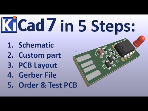
KiCAD 7 PCB Layout in 5 steps
 0:05:50
Tame the yellow line: Master KiCad 7 Edge.Cuts
 0:00:08
Received PCB From Various Manufacturers - KiCad 7 tutorial series #pcb #electronics
 0:04:50
#1 How To Use New Kicad 7.0 - Introduction | #PCBCupid
 0:00:07
Secret To Design A PCB in KiCad 7
 0:02:03
KiCad 6: Set Grid Origin
 0:01:31
Adding Libraries in Kicad
 0:06:30
#2 How To Use New Kicad 7.0 User Interface | #PCBCupid
 0:00:20
5V 18560 mAh Power Bank KiCAD | PCB Design & Development | 3D Model
 0:02:27
Apply eeschema placement to pcbnew/Kicad layout
 2:25:30
KiCad 7 ESP32 PCB Design Full Tutorial - made by morten laboratories iot-thing
 1:40:06
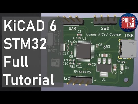
KiCad 6 STM32 PCB Design Full Tutorial - Phil's Lab #65
 0:00:20
5V 18560 mAh Power Bank KiCAD | PCB Design & Development | 3D Model
 0:00:31
H Bridge PCB Layout in 30 seconds using Kicad
 0:01:00
track has unconnected end(KiCad 6.0)
 0:12:40
#15 How To Optimize PCB in KiCad 7.0 For Beginners | #PCBCupid
 0:10:50
KiCAD 7 Autorouter – Simple Fast Prototyping
 0:11:13
#13 How To Create Custom Symbols in KiCad 7.0 With KLC | #PCBCupid
 0:00:12
smart vending machine #pcb #electronics #kicad #automation #diy #easyeda #robotautomation #schematic
 0:00:20
8051 Mini Development Board PCB Design in KiCAD
 0:00:59
KiCad 6: Add Track (Includes Hotkey!)
 0:18:23
KiCAD Tutorial #7: Getting started with the PCB Design
 0:13:16
KiCad 7 Update - Why KiCad?
Комментарии