EEVblog #1144 - Padauk Programmer Reverse Engineering

preview_player
Показать описание
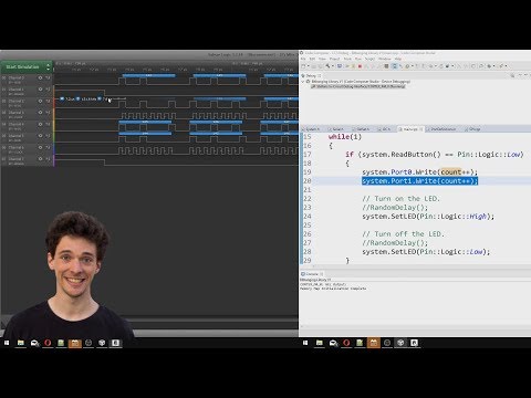
David looks at the pins on the Padauk PMS150 programmer for potential reverse engineering.
TLDR; It doesn't look easy to reverse engineer this protocol, it's messy with lots of voltage levels, as Padauk said it would be.
Just buy the programmer for now!
There is also a Flash/EEPROM re-programmable version of the chip, the PFS154C.

Support the EEVblog through Patreon!

Buy anything through that link and Dave gets a commission at no cost to you.

Stuff I recommend:

Donate With Bitcoin & Other Crypto Currencies!

Рекомендации по теме
Комментарии
Автор

>Something vaguely technical / tedious
"Get young Dave to do it"

pypes
Автор

I've reverse-engineered protocols in the past. Once because the authors of the protocol said they were too busy to provide documentation, another time because the documentation was lost. There is a certain satisfaction to sleuthing such things out.

marsgal
Автор

At 7:59 I think you're wrong. Rising edges are too close. I think data is read only on the falling edge. Create a sample program with a hex string of AA55AA55FF00FF00 then look for this data pattern. Thinking the slower clock cycles are the required time to burn each byte of data. Keep up the good work.

MichaelHagberg
Автор

I would assume that the voltage level change on the clock and data pins has no significance, they just have to adjust the logic levels as they change the Vcc. I.e. if you run a cmos logic chip on 10v, the 0->1 transition will happen at 5v; whereas it will happen at 2.5v if you run it on 5v. If I were you, I would look inside that programmer; maybe some labels / resistors can give some hints.

kunszabomarton
Автор

Instead of using this toy scope (only 8 ksample memory, seriously?) I would recommend to use one of Dave's good scopes, with megabytes of sampling memory, and 4 channels input. Would make reverse engineering much easier. The Keysight scopes have even the nice segmented memory feature, which allows you to sample multiple blocks with long pauses between, but still at high resolution for each block. You could probably record one full programming cycle with it.
The protocol for clock and data looks like SPI. With a Keysight scope you can also enable SPI decoding for selected channels, so that you don't have to manually decode the 0's and 1's, and then you can compare the numbers with the programming file to see where the actual programming starts. You could even read the scope memory over ethernet with SCPI commands to analyze the data further with e.g. Python script.

frankbuss
Автор

Keep it up David. Nothing rewarding ever comes easy. I like how you take us on the journey. Very down to earth.

RobTaylor-HiTech
Автор

In my opinion the best video of Dave2 so far :)

Momchil
Автор

I have seen programming patterns similar before. The programmer was sending data 'records' which contained various bits of information such as where the data was to be saved. This was then checked by the device using some sort of checksum. The programming voltage was then raised to allow the data record to be saved to the devices flash memory. It was similar to the way that a PIC self programs. Possibly the output pulses are some form of handshaking. It would be interesting to see what relation they have to the clock and data.

JerryWalker
Автор

Nice to see you are losing your nervousness and presenting yourself really well

timer
Автор

Maybe lower supply voltage for read cycles? Also have you generated a hex file to write 0x00-0xFF to see where the pattern shows up in the stream?

toddberg
Автор

In order not to lose the low voltage part in a logic analyzer capture, feed in the signal not through a resistive divider, but through a series resistor and a zener to ground after it. This will "cap" the high voltage signal down to the appropriate level while leaving the low voltage one unaffected (if capacitance of the zener screws up the rise and fall times, you can probably add a tiny capacitor in parallel with resistor to compensate).


The high supply voltage could be applied during the writing sessions in order to provide enough power to burn the fuses in the one-time-programmable memory.


Also, I think some Atmel MCUs have an alternative parallel programming mode that utilizes high programming voltage (you are supposed to use it if you've accidentally disabled RESET pin by setting fuse bits incorrectly). I'm not really into Atmel MCUs, so can't tell more specifically...


P.S. Did you notice there's exactly 8 bytes sent between each "chip select" line release?

SaNjA
Автор

very interesting!..crazy it has so many voltage levels.. i like your vids David..straight to the point and no BS!

WacKEDmaN
Автор

Very interesting, looking forward to the next installment! Cheers

SuprSi
Автор

I'm getting a very Bletchley Park vibe with this. Love it.

RemcoStoutjesdijk
Автор

This was really interesting. Looking forward to future videos about this.

jon_raymond
Автор

Use a beaglebone +beaglelogic. Will give you 100MHz logic analyzer up to 320MB samples. Also you can use an analog comparator from the supply voltage pin, so the threshold could follow the varying supply.

LucasHartmann
Автор

Just put a good logic analyzer on every pin for an unprogrammed chip and hit it with unique programming code and observe what happens.

Doompro
Автор

You could buffer the data line with an opamp, use a zener to limit the maximum voltage and put a comparator on the zener resistor to tell when the voltage is high. With multiple comparators you could even “digitize” the high voltage levels. It costs you some more pins, but at least you can use a normal logic analyzer

marvin
Автор

I watched the commercial at the end, instead of skipping it or clicking away. Support!

PhiTheProducer
Автор

I really enjoy videos like this. Keep em coming. Love to see what you figure out.

nate