filmov
tv
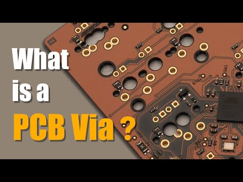
What is a PCB Via? | PCB Knowledge

Показать описание
In the multi-layer PCB design and manufacturing process, the term “via” is extensively used. However, what does the via mean, and how to use it in designs? In this video, we’ll cover some basics about the PCB via.
Chapters:
Intro 0:00
What is a Via? 0:16
Blind via 0:46
Buried via 1:11
Through-hole via 1:28
Tenting vias 1:46
Vias not covered 2:15
Plugged vias with solder mask 2:52
How to choose the via in my design? 3:12
Website:
Subscribe and follow us to keep updated with the latest news and promotion:
Chapters:
Intro 0:00
What is a Via? 0:16
Blind via 0:46
Buried via 1:11
Through-hole via 1:28
Tenting vias 1:46
Vias not covered 2:15
Plugged vias with solder mask 2:52
How to choose the via in my design? 3:12
Website:
Subscribe and follow us to keep updated with the latest news and promotion:
 0:03:52
What is a PCB Via? | PCB Knowledge
 0:02:15
What is a PCB Via? | Sierra Circuits
 0:17:01
PCB Vias 101 - Phil's Lab #77
 0:03:19
What are Stitching Vias? | PCB Knowledge
 0:05:27
How Do PCBs Work?
 0:18:54
How GND VIAs Improve Your PCB Layout
 0:03:09
Via-in-Pad Design | PCB Knowledge
 0:01:26
Connectivity of PCB Layers, vias on a home-made PCB
 0:03:03
What is a microvia hole in a PCB? | PCB design and technology
 0:02:39
Watch a high speed signal travel through your PCB | Simple Animation
 0:02:16
What type of via hole plugging in a PCB is recommended? | PCB design and technology
 0:10:27
What are PCBs? || How do PCBs Work?
 0:06:12
PCB Via
 0:08:30
Vias in PCB | Types of Vias | Through Hole , Blind & Buried Via
 0:15:55
Vias and Their Aspect Ratios | PCB Routing
 0:17:00
Stitching Via Deep Dive | PCB Layout
 0:11:32
#1421 PCB - Grounds
 1:19:29
How Does Copper Get Inside of a VIA Hole in Your PCB - Do you know this? (with Kailey Shara)
 0:03:47
Eagle PCB Tutorial | How to use via?
 0:03:22
What is PCB Back Drilling? | PCB Knowledge
 0:12:52
Top 5 Beginner PCB Design Mistakes (and how to fix them)
 0:14:47
Process 01: An open source 2 layer PCB process - part 1
 0:01:12
What is a via used in PCB? How to design?
 0:13:12
How PCB is Made in China - PCBWay - Factory Tour
Комментарии