filmov
tv
Process 01: An open source 2 layer PCB process - part 1

Показать описание
This video presents Process 01, an open source 2 layer PCB production process, including electroless copper plating of vias.
In this first part I will go through all the 31 steps required to make a double sided printed circuit board, while in the next video I will detail the preparation of all chemical solutions required by the process.
Other works cited in this video:
Example of 2 layer PCB without plated vias, using rivets:
Conductive graphite and electroplating process experiments:
Electroless copper plating experiments:
Images used in this video:
 0:14:47
Process 01: An open source 2 layer PCB process - part 1
 0:08:39
Process 01: An open source 2 layer PCB process - part 2
 0:03:58
Towards an open source 2 layer PCB process
 0:06:57
PLC vs Industrial Open-Source Controller (Arduino-Compatible) from AutomationDirect
 0:03:49
The Dark Side of Open Source // What really happened to Faker.js?
 0:00:15
Cosplay by b.tech final year at IIT Kharagpur
 0:00:16
How to Open a GitHub Repository in VS Code on Your Browser | Free web based code editor Trick 🔥
 0:00:24
Fast Food App in React Native 🔥 #shorts #reactnative #expo #reactjs #app #ui
 0:07:22
Portal 2 Mod - How to Make Your Composer GO Crazy // DEVLOG #1
 0:29:42
Papra: The Open-Source Document Manager You’ll Actually Use
 0:00:16
Making 1 Million by Legendary Paco Rabanne! #fragrance #perfume #pacorabanne #onemillion #shorts
 0:00:15
Trading for Beginners
 0:00:12
IIT Bombay Lecture Hall | IIT Bombay Motivation | #shorts #ytshorts #iit
 0:00:21
😱Viral Open Pores Home Remedy/Open Pores Treatment #shorts #skincare #youtubeshorts Anamika Barai
 0:03:18
Contributing to Open Source Can Change Your Life - Here’s How to Do It
 0:00:48
Why You Should Invest Early
 0:00:11
Timelapse of cute kittens from 1 day to 1 month #cat #kitten #kucinglucu #catlover #timelapse
 0:00:17
gold bar | gold biscuit | pure gold
 0:00:20
🤯 Pass any online exam with this Chat GPT extension (full video on channel 👇🏻)
 0:00:16
How to pinch the abacus in 5 seconds!
 0:00:29
IQ TEST
 0:00:40
How much does a PSYCHOLOGIST earn?
 0:00:22
Why YOU SHOULDN'T BUY The NEW Bugatti Bolide! 🤮
 0:00:20
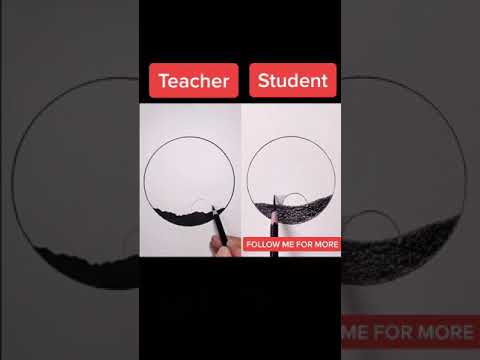
Teacher vs Student drawing challenge #drawing #art #12
Комментарии