filmov
tv
Field Effect Transistor Working in Tamil

Показать описание
FET- Field-Effect Transistor Construction and working principle of Operation.
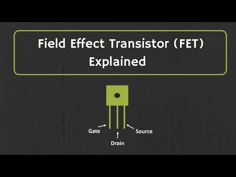
A Field Effect Transistor (FET) is a three-terminal semiconductor device. Its operation is based on a controlled input voltage. By appearance JFET and bipolar transistors are very similar. However, BJT is a current controlled device and JFET is controlled by input voltage. Most commonly two types of FETs are available.
Junction Field Effect Transistor (JFET)
Metal Oxide Semiconductor FET (IGFET)
Junction Field Effect Transistor
The functioning of Junction Field Effect Transistor depends upon the flow of majority carriers (electrons or holes) only. Basically, JFETs consist of an N type or P type silicon bar containing PN junctions at the sides. Following are some important points to remember about FET −
Gate − By using diffusion or alloying technique, both sides of N type bar are heavily doped to create PN junction. These doped regions are called gate (G).
Source − It is the entry point for majority carriers through which they enter into the semiconductor bar.
Drain − It is the exit point for majority carriers through which they leave the semiconductor bar.
Channel − It is the area of N type material through which majority carriers pass from the source to drain.
There are two types of JFETs commonly used in the field semiconductor devices: N-Channel JFET and P-Channel JFET.
N-Channel JFET
It has a thin layer of N type material formed on P type substrate. Following figure shows the crystal structure and schematic symbol of an N-channel JFET. Then the gate is formed on top of the N channel with P type material. At the end of the channel and the gate, lead wires are attached and the substrate has no connection.
When a DC voltage source is connected to the source and the drain leads of a JFET, maximum current will flow through the channel. The same amount of current will flow from the source and the drain terminals. The amount of channel current flow will be determined by the value of VDD and the internal resistance of the channel.
A typical value of source-drain resistance of a JFET is quite a few hundred ohms. It is clear that even when the gate is open full current conduction will take place in the channel. Essentially, the amount of bias voltage applied at ID, controls the flow of current carriers passing through the channel of a JFET. With a small change in gate voltage, JFET can be controlled anywhere between full conduction and cutoff state.
Thank you for watching
 0:08:29
How FETs Work - The Learning Circuit
 0:06:29
What is a JFET and how does it work?
 0:09:06
Construction and Working of JFET
 0:08:16
What is Field Effect Transistor (FET)? || Differences between BJT and FET || Types of FET
 0:11:07
Introduction to Field-Effect Transistors (FETs)
 0:12:17
Transistors - Field Effect and Bipolar Transistors: MOSFETS and BJTs
 0:12:09
Field Effect Transistor Working in Tamil
 0:16:19
JFET: Construction and Working Explained
 0:03:01
3 Automatic ON OFF Circuit
 0:04:16
JFET - Construction & Working - Easy Explanation - Electronics
 0:03:42
How MOSFETs and Field-Effect Transistors Work!
 0:04:43
How a MOSFET Works - with animation! | Intermediate Electronics
 0:18:20
JFET (Junction Field Effect Transistor) Working & Characteristics (Basic Electronics)
 0:08:13
How Does a MOSFET Work?
 0:07:08
What is FET (Field Effect Transistor) BJT Vs FET (Basic Electronics)
 0:11:03
Working of JFET (Zero Voltage at the Gate)
 0:00:33
What is a Field Effect Transistor?
 0:07:43
Working of Transistors | MOSFET
 0:05:46
Operation of JFET N - Channel - Field Effect Transistor - Basic Electronics
 0:20:14
MOSFET Explained - How MOSFET Works
 0:09:07
#14 n channel JFET working || EC Academy
 0:08:04
What is a Transistor | Working Principles
 0:08:02
#13 Introduction to FET || construction of FET (Field Effect Transistor) || Ec Academy
 0:02:22
how works N channel JFET -junction field effect transistor
Комментарии