filmov
tv
What is a JFET and how does it work?

Показать описание
Table of Contents
0:00 Introduction
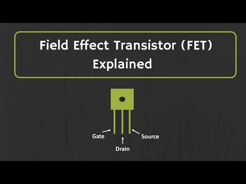
0:34 Parts of a JFET
0:50 JFET Symbol
1:20 How a JFET is built
1:50 Review of a PN Junction
2:33 Internal construction and function of a JFET
4:56 Comparison between JFET and MOSFET
5:22 Summary
CircuitBread is joining the fight to help people more easily learn about and use electronics. With an ever-growing array of equations, tools, and tutorials, we're striving for the best ways to make electronics and electrical engineering topics more accessible to everyone.
Connect with CircuitBread:
 0:06:29
What is a JFET and how does it work?
 0:09:06
Construction and Working of JFET
 0:08:29
How FETs Work - The Learning Circuit
 0:16:19
JFET: Construction and Working Explained
 0:02:33
What is a JFET | Junction Field Effect Transistor & its Polarities | Electronic Devices & Ci...
 0:04:16
JFET - Construction & Working - Easy Explanation - Electronics
 0:05:16
The VI Characteristics and Operating Regions of a JFET
 0:01:57
What is Transfer Characteristics of a JFET | Junction Field Effect Transistor | EDC
 1:03:51
January 3 Circuit Analysis Live
 0:08:16
What is Field Effect Transistor (FET)? || Differences between BJT and FET || Types of FET
 0:00:51
When would you use a JFET versus a MOSFET?
 0:06:18
What is JFET Transistör? How Does JFETs Work? (JFET Explained)
 0:00:54
Physical Topology of a JFET
 0:02:44
What is a Working Principle of JFET | N Channel & P Channel | Junction Field Effect Transistor |...
 0:00:33
VI Characteristics of a JFET
 0:05:45
what is jfet working principle # JFET # ELECTRONICS
 0:06:43
Very Basic Explanation of a JFET and a simple analogy to help you remember!
 0:16:51
Junction Field Effect Transistor (JFET) introduction and characteristics PT1
 0:08:26
Junction Field Effect Transistor, JFET - Structure, Output, Transfer Characteristic, Regions
 0:08:41
JFET and MOSFET
 0:03:46
Working of JFET | How JFET works? | JFET working animation
 0:05:37
What is JFET? Types and Working
 0:00:05
Basic differences between JFET & BJT💡 #shorts #youtubeshorts #electrical #electronics #eee
 0:00:55
PN Junction Hiding in a JFET
Комментарии