filmov
tv
JFET: Construction and Working Explained
Показать описание
In this video, the construction and working of n-channel JFET and p-channel JFET are explained.
By watching this video, you will learn the following topics:
1:01 Construction of n-channel JFET
2:25 Working of n-channel JFET
6:01 Output characteristics (Drain curves) of n-channel JFET
11:07 Different regions of operation of JFET
13:07 p-channel JFET
14:44 Symbols of n-channel and p-channel JFET
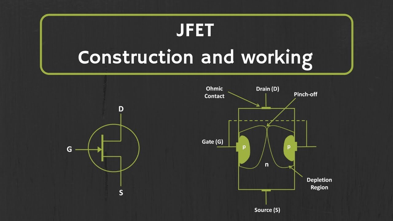
JFET (Junction Field Effect Transistor) :
The junction field Effect Transistor (JFET) is used in a wide range of applications. It is a three terminal device. (The 3 terminals are Gate, Drain, and Source)
JFET can be classified as either n-channel JFET or p-channel JFET.
n-channel JFET:
In the n-channel JFET, the channel is made up of n-type semiconductor material and two small p-type regions are formed near the channel.
p-channel JFET:
In the p-channel JFET, the channel is made up of p-type semiconductor material and two small n-type regions are formed near the channel.
In this video, the construction and working of JFET are explained by taking the example of n-channel JFET. And at the latter part of the video, the output characteristics (Drain curves) and the different region of operation of JFET is also discussed.
Different regions of operation of JFET:
1) Ohmic region
2) Saturation Region
3) Cut-off Region
4) Breakdown Region
This video will be helpful to all students of science and engineering in understanding the construction and working of JFET.
#JFET
#JFETWorking
#NchannelJFET
#PchannelJFET
Follow me on YouTube:
Follow me on Facebook:
Follow me on Instagram:
Music Credit:
By watching this video, you will learn the following topics:
1:01 Construction of n-channel JFET
2:25 Working of n-channel JFET
6:01 Output characteristics (Drain curves) of n-channel JFET
11:07 Different regions of operation of JFET
13:07 p-channel JFET
14:44 Symbols of n-channel and p-channel JFET
JFET (Junction Field Effect Transistor) :
The junction field Effect Transistor (JFET) is used in a wide range of applications. It is a three terminal device. (The 3 terminals are Gate, Drain, and Source)
JFET can be classified as either n-channel JFET or p-channel JFET.
n-channel JFET:
In the n-channel JFET, the channel is made up of n-type semiconductor material and two small p-type regions are formed near the channel.
p-channel JFET:
In the p-channel JFET, the channel is made up of p-type semiconductor material and two small n-type regions are formed near the channel.
In this video, the construction and working of JFET are explained by taking the example of n-channel JFET. And at the latter part of the video, the output characteristics (Drain curves) and the different region of operation of JFET is also discussed.
Different regions of operation of JFET:
1) Ohmic region
2) Saturation Region
3) Cut-off Region
4) Breakdown Region
This video will be helpful to all students of science and engineering in understanding the construction and working of JFET.
#JFET
#JFETWorking
#NchannelJFET
#PchannelJFET
Follow me on YouTube:
Follow me on Facebook:
Follow me on Instagram:
Music Credit:
 0:16:19
JFET: Construction and Working Explained
 0:09:06
Construction and Working of JFET
 0:04:16
JFET - Construction & Working - Easy Explanation - Electronics
 0:06:29
What is a JFET and how does it work?
 0:18:20
JFET (Junction Field Effect Transistor) Working & Characteristics (Basic Electronics)
 0:03:46
Working of JFET | How JFET works? | JFET working animation
 0:05:16
The VI Characteristics and Operating Regions of a JFET
 0:18:41
jfet (construction and working) | hindi
 0:06:32
Junction Field Effect Transistor [JFET] Explained: Construction, Working, Application | Shubham Kola
 0:05:46
Operation of JFET N - Channel - Field Effect Transistor - Basic Electronics
 0:11:03
Working of JFET (Zero Voltage at the Gate)
 0:09:07
#14 n channel JFET working || EC Academy
 0:15:45
JFET (Basics, Symbol, Structure, Working & Characteristics) Explained
 0:12:24
Working of JFET (N-channel) -1 || Telugu
 0:17:50
JFET: Construction and Working in Engllsh
 0:12:09
Field Effect Transistor Working in Tamil
 0:03:51
Junction Field Effect Transistor (JFET) - Construction
 0:31:18
JFET: Construction Working and Characteristics | Electronic Devices and Circuits - 1 in EXTC
 0:05:53
Classification of FET, Construction and Symbol of P and N channel FET - Basic Electronics
 0:01:00
Junction Field Effect Transistor : Construction of N Channel and P Channel JFET #shorts
 0:02:22
how works N channel JFET -junction field effect transistor
 0:08:23
Working of JFET (Negative Voltage at the Gate)
 0:11:07
Introduction to Field-Effect Transistors (FETs)
 0:07:08
What is FET (Field Effect Transistor) BJT Vs FET (Basic Electronics)
Комментарии