filmov
tv
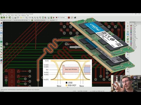
EEVblog #1216 - PCB Layout + FPGA Deep Dive

Показать описание
Only Dave can turn a simple question into a 1hr deep dive monologue into PCB layout and FPGA implementation.
FPGA power supplies, DC margins, dynamic power requirements, power budgets, high power designs, multi layer PCB design, placement, system considerations, power planes, copper weighting, stackups, routing, split planes, star grounding, blind and buried vias, high speed traces, return paths, EMC, and a whole lot more.
#FPGA #PCB #Design
Bitcoin Donations: 38y7DE8HEHNj8fGDtUr4PkCn9nWxiorvvy
Litecoin: ML7oQokTwB38bgzzjLDbRV97HKAHuwRfHA
Ethereum: 0x11AceA38DCA9DbFfB4F35f3F746af65F9dED28ce
Support the EEVblog through Patreon!
Buy anything through that link and Dave gets a commission at no cost to you.
Stuff I recommend:
Donate With Bitcoin & Other Crypto Currencies!
 0:59:18
EEVblog #1216 - PCB Layout + FPGA Deep Dive
 0:29:42
EEVblog 1559 - PCB Design: Trace Current Rating
 0:39:34
EEVblog #1247 - DDR Memory PCB Propagation Delay & Layout
 0:27:03
EEVblog #1327 - 3 Ways to FAIL at PCB Manufacture
 1:18:31
KiCAD PCB Design
 0:27:59
EEVblog #1211 - Apple's Most Beautiful Failure
 0:45:10
EEVblog #1365 - Viewer PCB & Circuit Design Review
 0:39:47
EEVblog #1221 - Mailbag Monday
 0:39:51
EEVblog #1222 - Apple's MacBook Design FAIL - Who's To Blame?
 0:25:41
EEVblog #1109 - Spectrum Analyser Design Walk-through
 0:07:28
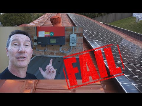
EEVblog #1217 - My Home Solar Power System FAILED!
 0:18:26
20 PCB Design Pitfalls
 0:48:46
EEVblog #1218 - 1GHz Oscilloscope Spec Shootout
 0:16:16
EEVblog #58 - Warm and Fuzzy FPGA Troubleshooting
 0:36:43
EEVblog #1241 - Power Up Display Counter Project - Part 1
 0:29:56
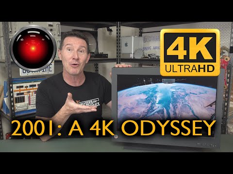
EEVblog #1215 - $18,000 4K Monitor Teardown From 2001!
 0:46:27
EEVblog #1229 - Mailbag
 0:49:13
EEVblog #1201 - Nobel Laureate in the EEVBlog Lab!
 0:29:57
EEVblog 1430 - Rent vs Buy - My $400,000 MISTAKE!
 0:17:01
IBM BGA Thermal Futility...
 0:19:46
EEVblog #1207 - ARM Dev Boards Falling From The Sky!
 0:42:34
EEVblog #1209 - Mailbag
 0:17:00
EEVblog #1213 - The Oscilloscope Interpolation Trap!
 0:41:01
EEVblog #1203 - REPAIR: Tektronix 2465B Oscilloscope
Комментарии