filmov
tv
Silicon semiconductor manufacturing process

Показать описание
Semi-conductive silicon wafer dicing,grinding and processing
A wafer is a thin slice of semiconductor material used to fabricate integrated circuits or other microdevices1. Also called a slice or substrate, wafers must undergo a number of steps in the preparation process before they are ready for use.
Manufacturing processes for silicon semiconductor
Silicon Ingot ⇒ Cropping(electroplated bandsaw) ⇒ Cylindrical / Flat Grinding Silicon Rod ⇒ Ingot Silicon (diamond wire) ⇒ Lapping (double side wheel/polishing pad) ⇒ Edge Grinding ⇒ Surface grinding ⇒ polishing⇒ wafer⇒ patterning ⇒ back grinding (vitrified / resin wheels) ⇒ dicing (dicing blades)⇒ chips ⇒ molding ⇒ packaging
More Superhard provides diamond tools for the semiconductor industry including
► Diamond Bandsaw Blades
Cutting silicon ingot in semiconductor industry. They are also cut sapphire ingot , quartz glass, etc
Edge shapes diamond bandsaw blades: continuous, segmented ( half moon) and serrated shape
► Cylindical / Surface Grinding Wheels
Peripheral grinding of silicon ingots, or processing the outer surface of silicon ingots and to make orientation flat
► Edge Grinding Wheel
Edge wheel/ chamfering wheels for silicon and sapphire wafer edge grinding. A small diamterer wheel for notch grinding
► Dicing Blades ( Hub type and Hubless type)
Ultra - thin diamond dicing blade ( hub type and hubless type) for scribing silicon wafers, compound semiconductor wafers (GaAs, Gap)
► PU Polishing Pad
Polishing and finishing of glass, LCD/LED substrates, precision optics, hard disk, metal and semiconductor wafer surfaces
 0:07:44
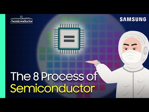
‘Semiconductor Manufacturing Process’ Explained | 'All About Semiconductor' by Samsung Sem...
 0:02:05
Semiconductor production process explained
 0:05:35
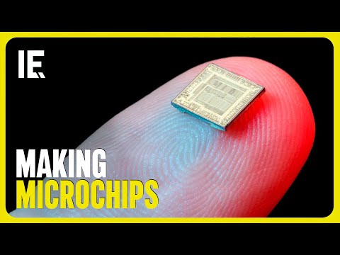
💻 How Are Microchips Made?
 0:27:48
How are Microchips Made? 🖥️🛠️ CPU Manufacturing Process Steps
 0:00:26
Silicon semiconductor manufacturing process
 0:04:20
#300mm Silicon #Wafer Manufacturing Process
 0:08:40
How are BILLIONS of MICROCHIPS made from SAND? | How are SILICON WAFERS made?
 0:09:21
How Are Semiconductor Chips Made?
 0:00:52
Creating A Silicon Wafer - How Sand Becomes Computers (1 of 6)
 0:00:56
How microchips are made
 0:05:29
How are microchips made? - George Zaidan and Sajan Saini
 0:23:01
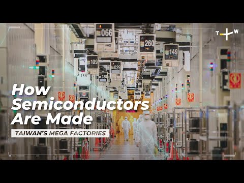
Inside Micron Taiwan’s Semiconductor Factory | Taiwan’s Mega Factories EP1
 0:01:00
An interesting #AMD silicon wafer
 0:22:26
Doping: The Most Important Part of Making Semiconductors
 0:21:29
What Goes On Inside a Semiconductor Wafer Fab
 0:00:41
Creating Circuits On A Silicon Wafer - How Sand Becomes Computers (2 of 6)
 0:05:25
Uncovering the Silicon: Demystifying How Chips are Built and How They Work
 0:01:40
How To Make A CPU
 0:05:46
'Z2' - Upgraded Homemade Silicon Chips
 0:02:42
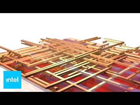
Intel: The Making of a Chip with 22nm/3D Transistors | Intel
 0:08:01
Silicon: The Cleverest Element On Earth
 0:04:21
How Silicon Wafers Are Made: 🔬From Sand to Smartphone Power📱#siliconwafers #semiconductor #wafer...
 0:03:48
THE SEMICONDUCTOR SUPPLY CHAIN - A BRIEF OVERVIEW
 0:00:30
The Art of Semiconductor Manufacturing #shorts | The Wealthy Web
Комментарии