filmov
tv
Making Tiny Things with Electron Microscope - E-beam Lithography

Показать описание
 0:08:44
Making Tiny Things with Electron Microscope - E-beam Lithography
 0:28:37
The World's Smallest Scanning Electron Microscope
 0:02:41
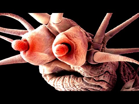
Objects Under Electron Microscope (Part 3)
 0:04:40
DIY Electron Accelerator - Cathode Ray Tube
 0:01:46
Making the Very Small, Big: The Electron Microscope - Stuff of Genius
 0:14:05
Shooting an electron beam through air
 0:19:54
How do Electron Microscopes Work? 🔬🛠🔬 Taking Pictures of Atoms
 0:02:28
New Objects Under Electron Microscope
 0:00:10
chemiosmosis and the electron transport chain
 0:14:57
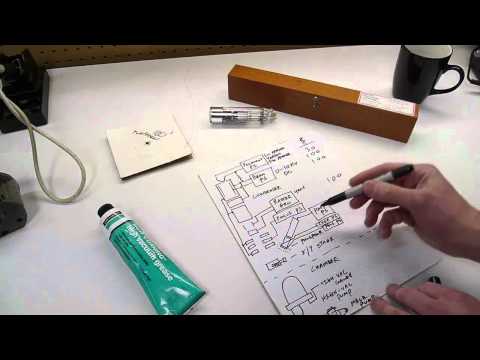
DIY Scanning Electron Microscope - Overview
 0:11:39
DIY Scanning Electron Microscope - Sources, Costs and References
 0:00:33
Until now, there are still factories producing electron tubes in small quantities. #facts
 0:00:49
How small is an Electron🤔 Neil deGrasse Tyson Explained #physics #science #atoms
 0:05:35
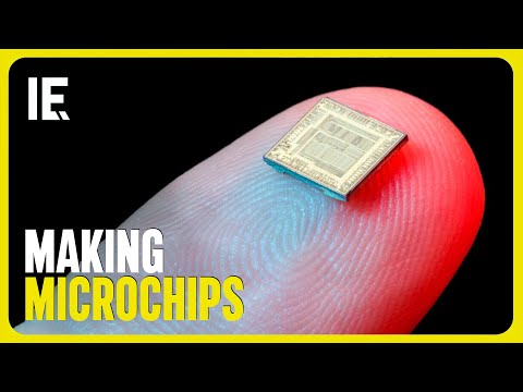
💻 How Are Microchips Made?
 0:00:13
Virus and bacteria under electron microscope
 0:02:32
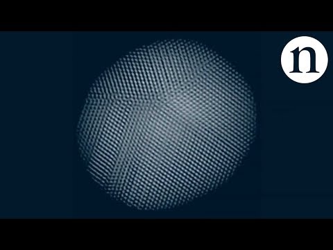
Have you ever seen an atom?
 0:00:32
How Do Electron Microscopes Work?
 0:09:52
DIY Scanning Electron Microscope - Operation procedure
 0:14:32
DIY Scanning Electron Microscope - Electron Gun Detail
 0:00:18
LaB6 Crystal Electron Beam Source
 0:01:49
Electron JS in 100 Seconds
 0:06:31
What Does an Electron Look Like?
 0:00:40
The Real Video of an Electron Captured For the First Time!!
 0:01:29
Zooming into an iPhone CPU Silicon Die using Electron Microscope
Комментарии