filmov
tv
The World's Smallest Scanning Electron Microscope

Показать описание
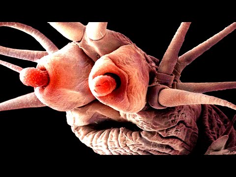
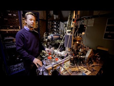
I got a chance to try out the world's smallest scanning electron microscope. But, not everything went according to plan. In theory, this machine is pretty awesome - it's portable and small enough to fit in the overhead compartment. It uses an iPad as the user interface, which is pretty intuitive. But it's just never worked well for me, because I'm at a higher altitude than the manufacturer has ever tested it, which has caused all sorts of problems with high voltage arcing.
0:00 Intro
2:07 Preparing an iPhone
5:27 How does an SEM work?
6:50 iPhone MEMS microphone
10:06 iPhone accelerometer
13:20 iPhone gyroscope
14:40 Metal coating
16:31 Cardboard
17:32 Thermal camera sensor
22:30 Challenges of making this video
A huge thank you to everyone that helped with the video. The manufacturer, the experts that advised me, and everyone that sent in things to look at. We all worked incredibly hard to make this a success, and I'm really sad we couldn't get the machine to behave.
See behind the scenes at Strange Parts:
Music:
 0:28:37
The World's Smallest Scanning Electron Microscope
 0:01:34
A Boy And His Atom: The World's Smallest Movie
 0:02:41
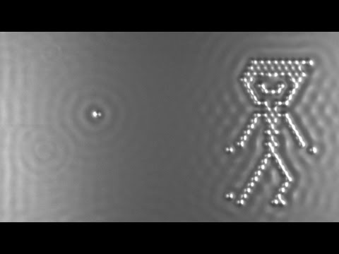
Objects Under Electron Microscope (Part 3)
 0:10:09
The World's Smallest 'Pewdiepie'—The Microscopic Writing Experiment
 0:03:01
Objects Under Electron Microscope [Part 4]
 0:23:40
50,000,000x Magnification
 0:02:28
New Objects Under Electron Microscope
 0:02:02
Voyage into the world of atoms
 0:05:50
Seeing the Smallest Thing in the Universe
 0:04:56
Moving Atoms: Making The World's Smallest Movie
 0:18:25
Amazing Electron Microscope Images
 0:00:59
World's smallest scanning electron microscope (SEM). # Aaron Huey
 0:00:40
The Smallest Word Written With Electrons
 0:05:51
The World’s Highest Resolution Electron Microscope - Hitachi
 0:02:19
The Clearest Image of An ATOM
 0:00:38
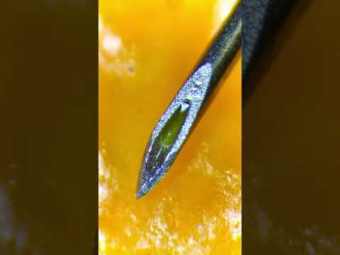
Used syringe under the microscope is insane (real!)
 0:00:56
Smallest Electron Microscope
 0:01:34
A Boy And His Atom: The World's Smallest Movie - Unravel Travel TV
 0:03:20
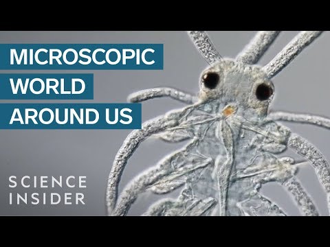
Award-Winning Footage Of The Microsopic World Around Us
 0:04:39
The World’s Smallest MRI (Nature Physics)
 0:00:48
How small are atoms?
 0:05:35
A Better Way To Picture Atoms
 0:07:09
Microscopic view of an Intel i486
 0:00:55
LARGEST TESLA COIL IN THE WORLD (3 million volts discharged)
Комментарии