filmov
tv
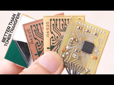
DIY PCBs At Home (Single Sided Presensitized)

Показать описание
Learn to fabricate Single Sided PCBs at home! Prototype PCB fabrication is one of the essential skills you must learn in electronics. Instead of using breadboards and perfboards, custom PCBs would make any project smaller and more compact!
PRESENSITIZED PCBs:
Also known as photopositive PCBs or photoresist PCBs, are regular PCB copper clads, layered with a light sensitive paint or film. Once exposed to light, the paint would dissolve in the developing solution, while the unexposed areas would remain undissolved in the solution. This forms a Mask on the clad. When the developed PCB is exposed to an etchant, the masked areas would remain in tact while the unmasked areas would dissolve on your etchant, thus forming a copy of your printed PCB artwork.
WHAT PAPER AND PRINTER TYPE TO USE:
- You can use an injket printer for this type of PCB fabrication, no need for toner printers.
- I use regular Short Bond Paper (Letter 8.5x11"). You can use parchment paper or inkjet friendly films for better fabrication quality.
BETTER THAN TONER TRANSFER METHOD:
Toner transfer method has been the number 1 go to in homebrew PCB fabcrication, next to the sharpie method. Toner transfer has its own limitations. One, is that you would need a toner printer, common inkjet printers simply wouldn't work. Second, as your line traces gets thinner, it would be more difficult to transfer the toner prints to the copper clad. Presensitized PCBs on the other hand creates the sharpest lines of all the homebrew fabrication methods. This is perfect for smaller circuits that involves SMT (Surface Mount) components. I use this method for building PCBs with line traces reaching down to 10mils (0.254mm). You can go as thin as 5mils (0.1275mm), but you would have to use inkjet friendly acetate.
_______________________________
Instructable Tutorial:
DIY Etching PCB Shaker
DIY Digital PCB Exposure Box!
_______________________________
Tools & Materials:
1.) Photopositive PCB Pack
2.) Ferric Chloride (Copper Etchant)
3.) Pure Acetone (Nail Polish Remover)
4.) Baby Oil
5.) Mini Drill
6.) Drill Bits (0.8mm - 1.0mm)
7.) LED/ CFL/ UV Lamp
8.) Cutter Knife
9.) Hack Saw
10.) Wooden Plank
#Circuits #Electronics #DIY , Kinsten PCB
 0:10:11
DIY PCBs At Home (Single Sided Presensitized)
 0:12:23
You can now PRINT PCBs! Creating a homemade PCB with the Voltera V-One PCB Printer!
 0:05:35
DIY PCB Fabrication (Dry Film Inkjet Method)
 0:10:56
The fastest way to make crisp PCBs at home!
 0:10:04
How to make HIGH quality PCBs at home
 0:04:38
Making of PCBs at home, DIY using inexpenive materials
 0:06:17
The fastest way to make crisp PCBs at home! DIY PCB Fabrication
 0:10:40
PCB Creation for Beginners - Start to finish tutorial in 10 minutes
 0:12:29
'A Machine PERFECT for Making PCBs at Home' Is what they said!
 0:45:41
High Quality DIY PCB Boards at Home, Step by Step detailed Instructions (PLUS SMD SOLDERING)
 0:04:35
Homemade PCB Etching (through hole parts) - Part 1
 0:12:09
The fastest way to make PCBs at home - UV MSLA Printer
 0:06:41
Easy Vias on Home PCBs
 0:44:57
Homemade PCBs with Fiber Laser - 0.1mm Clearance
 0:40:27
Make A Circuit Board, At Home!
 0:11:05
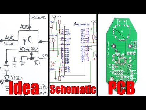
From Idea to Schematic to PCB - How to do it easily!
 0:08:08
Printing PCBs At Home!
 0:08:51
How to Make A PCB Making CNC in Your Budget
 0:05:49
How to Solder Mask PCBs #Adafruit
 0:00:56
3D Printing 4-layer PCBs with BotFactory SV2
 0:18:04
TUTORIAL: How to Make Your Own DIY PCBs! - Part 1 - Quick, Cheap & Easy! (Toner, Acetone & N...
 0:34:27
Make custom PCBs with the Sienci CNC and FlatCAM!
 0:07:51
Make professional PCBs at home
 0:11:29
The Best way to Solder? Hot Plate to the rescue! (DIY or Buy)
Комментарии