filmov
tv
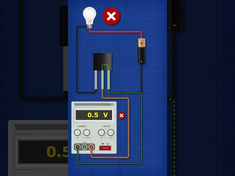
Working of JFET (Negative Voltage at the Gate)

Показать описание
Analog Electronics: Working of JFET (Negative Voltage at the Gate)
Topics Covered:
1. Working of junction field effect transistor.
2. Working of JFET when the voltage between gate and source is negative (or less than zero) and the voltage between drain and source is greater than zero.
3. Effect on depletion region.
Topics Covered:
1. Working of junction field effect transistor.
2. Working of JFET when the voltage between gate and source is negative (or less than zero) and the voltage between drain and source is greater than zero.
3. Effect on depletion region.
 0:08:23
Working of JFET (Negative Voltage at the Gate)
 0:07:45
Working of JFET for negative Gate voltage
 0:03:37
Working of JFET (Negative Voltage at the Gate)
 0:16:19
JFET: Construction and Working Explained
 0:09:17
Lecture 5-working of JFET (NEGATIVE VOLTAGE AT GATE)
 0:11:03
Working of JFET (Zero Voltage at the Gate)
 0:05:16
The VI Characteristics and Operating Regions of a JFET
 0:06:29
What is a JFET and how does it work?
 0:15:25
Working of JFET ( Negative voltage at a Gate terminal)
 0:08:49
Working of FET with negative gate to source voltage in Tamil I Electron devices in Tamil
 0:11:25
Semiconductor Devices: JFET Voltage Controlled Resistor
 0:14:59
Output or Drain Characteristics of JFET
 0:09:06
Construction and Working of JFET
 0:15:38
Exploring How JFETs (Junction Field-Effect Transistors) Work! - DC to Daylight
 0:04:16
JFET - Construction & Working - Easy Explanation - Electronics
 0:07:31
Characteristics of JFET - Field Effect Transistor - Basic Electronics
 0:08:58
6 Ways: How to Convert a Positive Input Voltage into a Negative Output Voltage
 0:18:13
🔴 JFET (PART 2) - Negative voltage in GATE || for B.Sc. in HINDI
 0:17:15
Effect of Depletion Region, Output or Drain Characteristics, Transfer Characteristics of JFET
 0:13:27
jfet construction and working (for negative gate source voltage)
 0:01:00
Transistors Explained - What is a transistor?
 0:12:43
Why do Junction Transistors Amplify Current and not Voltage
 0:00:55
PN Junction Hiding in a JFET
 0:18:20
JFET (Junction Field Effect Transistor) Working & Characteristics (Basic Electronics)
Комментарии