filmov
tv
Altium Designer 21 - Using Polygons on Power Planes

Показать описание
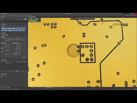
Traditionally, a PCB power plane is designed as a negative, that is, the objects placed on a power plane layer become voids in the copper when the board is fabricated. This approach is used because it is more efficient to generate the output data this way, as the bulk of a plane layer is normally copper; voids in the copper are only needed in specific locations such as around non-connected pads, or as separation voids when the plane is divided into different voltage regions.
As part of improving support for more complex power plane design, this release sees the addition of support for defining power planes as polygons. This change does not affect the approach to designing a power plane; they are still defined in the negative - so placing an object creates a void in the copper, and they continue to be split into separate regions by placing a split line. By using polygons, copper islands, narrow necks and dead copper can automatically be detected and removed.
Subscribe to our channel and remember to LIKE and SHARE.
 0:01:05
 0:00:47
 0:59:55
 0:06:23
 0:01:10
 0:09:50
 0:01:05
 0:01:05
 0:02:03
 0:00:57
 0:01:05
 0:09:24
 0:59:55
 0:00:33
 0:02:49
 0:00:44
 0:00:49
 0:16:21
 0:09:41
 0:01:10
 0:09:50
 0:36:34
 0:01:00
 0:00:42