filmov
tv
Basic logic gate outputwaveform/logic design/ digital electronics/ universal logic gate

Показать описание
Please subscribe my channel using gmail or hotmail or any other email id, don't subscribe it using your university/college email id. because it will not count.
Draw the output timing diagram of Three Input NAND Gate. When a not gate is connected at the output of AND gate or inverted output of AND gate called NAND gate. This operation is called the NAND operation.
Other videos
The output of Three Input NOR Gate when All Inputs are in waveform form
Draw the output timing diagram of Three Input NAND Gate. When a not gate is connected at the output of AND gate or inverted output of AND gate called NAND gate. This operation is called the NAND operation.
Other videos
The output of Three Input NOR Gate when All Inputs are in waveform form
 0:05:10
Basic logic gate outputwaveform/logic design/ digital electronics/ universal logic gate
 0:10:49
Output waveform of basic logic gate / digital logic design
 0:03:18
Basic logic gate timing diagram/ waveform of basic logic gate/digital electronics
 0:02:20
Waveforms of Basic Logic Gates | Digital Logic Design | Digital Electronics | Undergrad Academy
 0:07:28
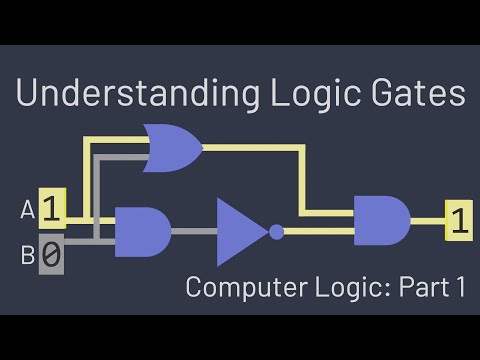
Understanding Logic Gates
 0:09:01
Output waveform of basic logic gate / digital logic design
 0:08:59
Types of Logic Gates | Symbols | Truth Tables
 0:05:42
Logic Circuit Analysis using Truth Tables
 0:04:21
Basic Logic Gate Output Waveform/XOR and XNOR gate/Digital Logic Design
 0:05:12
logic circuit Waveform/ Basic gate output waveform/OR Gate Output Waveform
 0:06:42
Logic gate circuit diagram output waveform/ Digital logic design/ Digital Electronics
 0:04:22
Logic gate timing diagram /output waveform of basic logic gates/digital electronics
 0:00:47
Output waveform of AND gate | Output Waveform of OR gate | logic gates
 0:09:01
output waveform of logic gate circuit diagram /Basic Logic Gate output waveform (Hindi)
 0:10:18
Digital Logic Circuit Design by Given input and Output waveform/ Digital Logic
 0:22:10
Diode Logic Gates - OR, NOR, AND, & NAND
 0:10:38
Timing diagram of basic logic gates/ 2 input, 3 input and 4 input logic gate (NAND)
 0:05:25
Logic Gates GATE Problem Example
 0:03:48
Output Waveform of NAND Gate/ Basic logic gate output waveform/Digital electronics
 0:04:23
Combinational Logic with Pulsed Waveforms
 0:04:54
(hindi) Logic Circuit Waveform Basics: Or Gate Output Waveform
 0:05:30
Basic OR Logic Gate Output Timing Diagram/ Digital Logic
 0:06:08
Physics: Logic Gates: Waveforms
 0:05:01
Basic Timing Diagrams for Combinational Logic Circuits
Комментарии