filmov
tv
Basic logic gate timing diagram/ waveform of basic logic gate/digital electronics

Показать описание
This video is on basic logic gate timing diagram. AND logic gate output timing diagram is drawn when both the input timing diagram is given. The timing diagram of both the input A and B are applied as input to AND gate. The output timing diagram of F is drawn for inputs.
 0:03:18
Basic logic gate timing diagram/ waveform of basic logic gate/digital electronics
 0:05:01
Basic Timing Diagrams for Combinational Logic Circuits
 0:02:20
Waveforms of Basic Logic Gates | Digital Logic Design | Digital Electronics | Undergrad Academy
 0:03:39
Basic Timing Diagrams
 0:26:23
Timing Diagrams (Digital Logic Tutorial) - Truth Table, Boolean expression as a Waveform, Explained
 0:05:39
Gate Delay and Timing Diagrams
 0:07:18
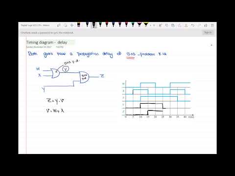
Timing diagram of the circuit with propagation delay
 0:54:07
Logic Gates, Truth Tables, Boolean Algebra AND, OR, NOT, NAND & NOR
 0:04:22
Logic gate timing diagram /output waveform of basic logic gates/digital electronics
 0:05:42
Logic Circuit Analysis using Truth Tables
 0:05:44
Basic logic gate timing diagram: Three input NAND Gate
 0:05:30
Basic OR Logic Gate Output Timing Diagram/ Digital Logic
 0:10:38
Timing diagram of basic logic gates/ 2 input, 3 input and 4 input logic gate (NAND)
 0:10:49
Output waveform of basic logic gate / digital logic design
 0:17:58
wave forms of basic logic gates (basic timing diagrams)
 0:08:59
Types of Logic Gates | Symbols | Truth Tables
 0:15:33
4.5 - Timing Hazards & Glitches
 0:09:01
Output waveform of basic logic gate / digital logic design
 0:11:11
Boolean Algebra & Logic Gates EP.1 - Truth Table & Timing Diagram
 0:04:24
Output timing diagram of basic logic gate (Four Input NAND Gate)
 0:05:28
Logic Gates - AND Gate Symbol Truth table Timing Diagram Waveform Explained in English
 0:13:58
Timing Diagram and Static '1' Hazard Elimination
 0:05:10
Basic logic gate outputwaveform/logic design/ digital electronics/ universal logic gate
 0:05:33
Logic gates wave forms problems
Комментарии