filmov
tv
Underwater laser cutting and silver sintering to make ceramic circuit boards

Показать описание
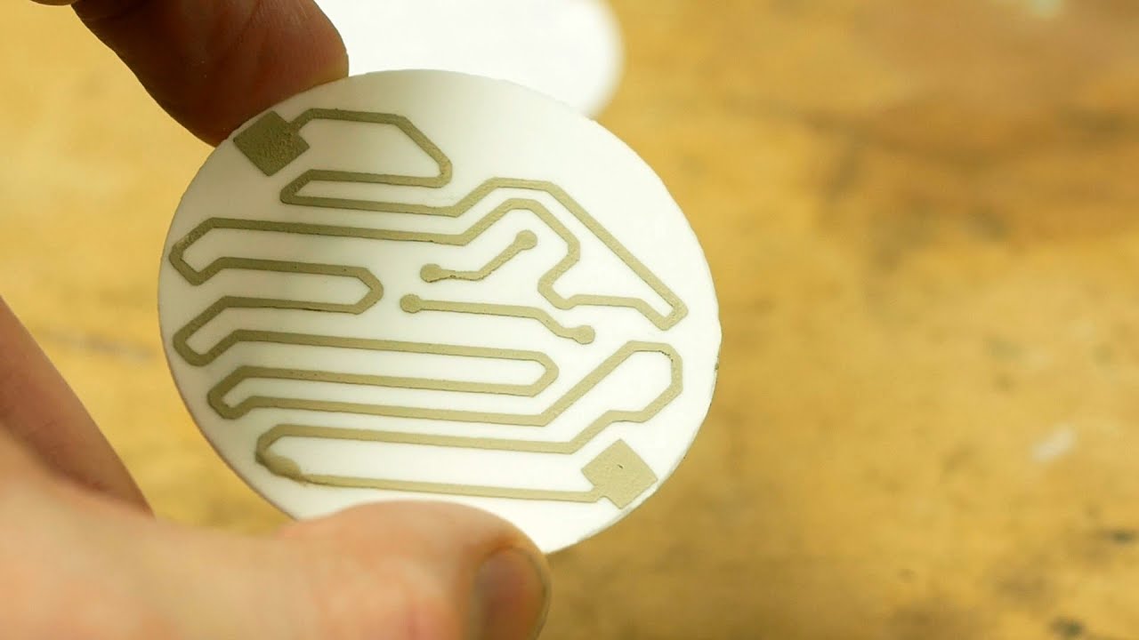
Thermal stress cracking can be completely avoided by CO2 laser cutting thin alumina sheets underwater. I also show how to formulate and apply silver paste, then sinter in a kiln to produce double-sided ceramic printed circuit boards with conductive vias.
60W CW CO2 laser at 80% power. 10mm/sec. Standard lens focal length (50mm). 2mm water above ceramic. 180 passes to cut through 0.75mm thick alumina.
Silver paste: 97% silver powder, 3% glass powder by mass. Particle size 1 micron or less. Add poly vinyl alcohol mold release until desired consistency reached.
Paste applied with 4 mil thick vinyl stencil. Dried in air 10 minutes, then rapidly brought up to 900*C, held for 10 minutes, then rapidly brought back down to room temperature. Total cycle about 45 minutes.
I measured electrical conductivity of the finished traces from my process with vinyl stencils: 4 milliohms per square at 10 micron final thickness. This is pretty close to the Dupont published spec ( less than 2 milliohm/sq at 16 micron thick)
Underwater laser cutting and silver sintering to make ceramic circuit boards
Avonisys waterjet laser technology / Precision ceramic and metal laser cutting
Laser Beam Strikes A House💥 #technology #space #laser #shorts #solareclipse #totalsolareclipse #sun...
20W Fiber Laser Beam Visualized Underwater
micro laser cutting
There’s always a bigger fish ! #shorts #creepy #magnapinna #surrealism #surreal #thalassophobia
Fiber laser cutting for Ceramics
2023 New Handheld Laser Welding Machine
Be Careful if You See one of These! #shorts
Underwater laser welding stainless steel
Titanium Tube - Fibre Laser Cutting
Can Fiber Laser Cutting Aluminum Sheet?
Extreme slow motion of a bullet through this thing
ATCLB-025025-150P Laser Cutting Ceramic and Alumina
Corte Laser / Laser Cut
🎙 Ben Krasnow, Applied Science // Hackster Café
500W Metal Sheet Fiber Laser Cutting Machine Cutting Show
Laser cutting machine cutting 12mm CS 20°V
Satisfying High Pressure Water Jet Cutting #shorts
Underwater Dance 😳 Mermaid 🧜🏻♀️ Merman - Choreography #shorts
amazing welding method of Pakistani welder #welding #shorts
I Saw Elon Musk Driving a Cyber Truck!! #Shorts
FREEDIVING COMPETITION BLACKOUT
The super glue idea that not many people know about
Комментарии
 0:23:16
 0:02:25
 0:00:05
 0:07:55
 0:00:10
 0:00:27
 0:00:52
 0:00:20
 0:00:38
 0:00:13
 0:00:47
 0:00:30
 0:00:16
 0:02:30
 0:00:30
 0:47:35
 0:01:59
 0:00:38
 0:00:45
 0:00:16
 0:00:34
 0:00:31
 0:00:33
 0:03:50