filmov
tv
How To Create Your Own Libraries in Altium Designer

Показать описание
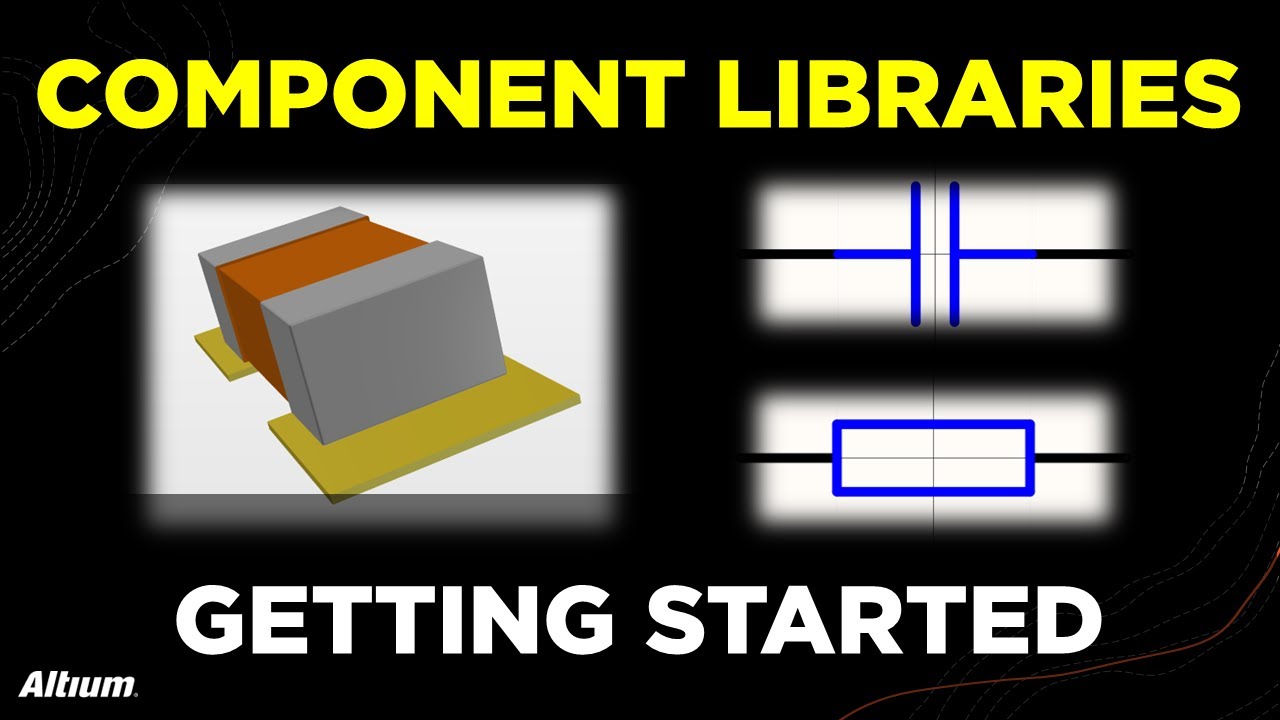
Learn how to create your own schematic symbols and footprints from scratch using Altium Designer.
Philip Salmony, Tech Consultant for Altium and the mind behind Phil's Lab, guides you through creating libraries including how to use the IPC-compliant footprint wizard to create a resistor and a capacitor.
What You'll Learn:
- Steps for CREATING SCHEMATIC libraries
- Tips for managing your own ALTIUM SCHEMATIC libraries
- How to design and link footprint libraries
- Tips for maintaining a clean and efficient design workflow
- Practical examples with resistors and capacitors
👉 Check Out Phil's Channel Phil's Lab: @PhilsLab
Don't forget to follow us on social to stay up-to-date on the latest Altium Academy content.
The Altium Academy is an online experience created to bring modern education to PCB Designers and Engineers all across the world. Here you can access a vast library of free training and educational content covering everything from basic design to advanced principles and step-by-step walkthroughs. Join industry legends as they share their career knowledge, review real-life design projects, or learn how to leverage one of Altium's leading design tools. No matter your level of experience, the Altium Academy can help you become a better Designer and Engineer!
About Altium LLC
Altium LLC (ASX:ALU), a global software company based in San Diego, California, is accelerating the pace of innovation through electronics. From individual inventors to multinational corporations, more PCB designers and engineers choose Altium software to design and realize electronics-based products.
#Altium #PCBdesign #electronicstutorial
0:00 Introduction
1:31 Creating Schematic Symbol Library
2:32 Resistor Symbol
7:27 Creating Footprint Library
7:53 Resistor Footprint (IPC Wizard)
11:31 Linking Footprint with Schematic Symbol
12:04 Capacitor Symbol
13:44 Capacitor Footprint (IPC Wizard)
15:45 Using Components in Project
16:40 Outro
Комментарии
 0:00:45
 0:09:33
 0:09:47
 0:14:52
 0:12:12
 0:00:31
 0:01:55
 0:03:27
 0:02:07
 0:22:33
 0:29:27
 0:23:33
 0:05:37
 0:06:57
 0:03:03
 0:03:48
 0:00:47
 0:13:22
 0:00:24
 0:08:11
 0:08:36
 0:09:29
 0:06:00
 0:06:17