filmov
tv
What is Reverse bias PN Junction Diode?

Показать описание
#short
reverse biasing of pn junction diode
effect on depletion layer
effect on potential barrier
reverse biasing of pn junction diode
effect on depletion layer
effect on potential barrier
 0:05:45
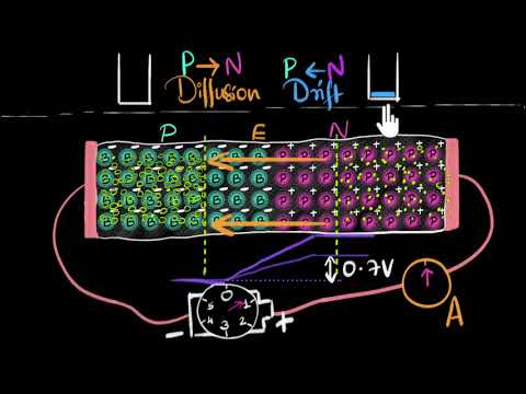
Reverse biasing a PN junction | Class 12 (India) | Physics | Khan Academy
 0:03:28
How does a reverse biased diode work at the molecular level? - Part 3 | Intermediate Electronics
 0:03:51
What is Reverse Biased p-n Junction Diode | Electronic Devices & Circuits | Engineering Concepts
 0:14:50
PN junction Diode Explained | Forward Bias and Reverse Bias
 0:06:37
Animation | How a P N junction semiconductor works | forward reverse bias | diffusion drift current
 0:06:32
PN Junction Reverse Biasing in tamil
 0:04:11
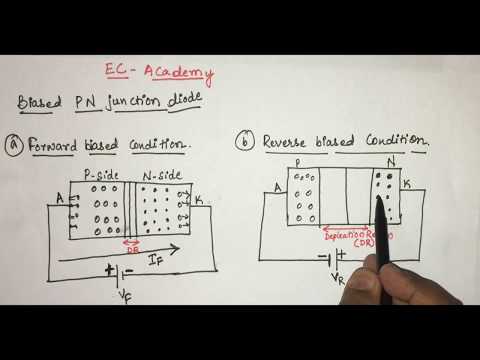
#3 P N junction diode under forward bias and reverse bias Condition || EC Academy
 0:00:59
What is Reverse bias PN Junction Diode?
 0:00:41
Reverse biasing of a P-n junction diode Animation
 0:10:26
Reverse Biased P-n Junction || Reverse Biase Characteristics || 2nd Year Physics - Chapter # 18
 0:03:29
P-N Junction with reverse biased explained in telugu .
 0:03:32
Reverse Biased P-N Junction Diode - Semiconductor Diode - Basic Electronics
 0:11:50
Forward and reverse current mechanism | Class 12 (India) | Physics | Khan Academy
 0:11:40
Photodiodes - (working & why it's reverse biased) | Semiconductors | Physics | Khan Academy
 0:02:35
What is p-n Junction Diode | Forward Bias & Reverse Bias | Electronic Devices & Circuits
 0:13:21
Forward Bias & Reverse Bias | Electronics
 0:06:50
Forward biasing a PN junction | Class 12 (India) | Physics | Khan Academy
 0:14:43
Reverse Bias (P N Junction Diode) Diode theory & applications (Basic Electronics)
 0:06:02
What is a Diode? - Forward and Reverse biased diode
 0:02:39
Reverse Biased PN Junction Diode || Reverse Biasing in Diode || PN Junction Biasing?? || Tamil
 0:05:34
Semiconductors 2: the p-n junction (Higher Physics)
 0:14:06
Diodes - What Are Diodes - PN Junction - Forward Bias - Reverse Bias - Zener Diodes
 0:15:57
56. Forward Bias & Reverse Bias Diode | Semi Conductors | Physics Baba 2.0
 0:06:53
PN Junction Biasing | Basic Electronics | Malayalam
Комментарии