filmov
tv
Forward biasing a PN junction | Class 12 (India) | Physics | Khan Academy

Показать описание
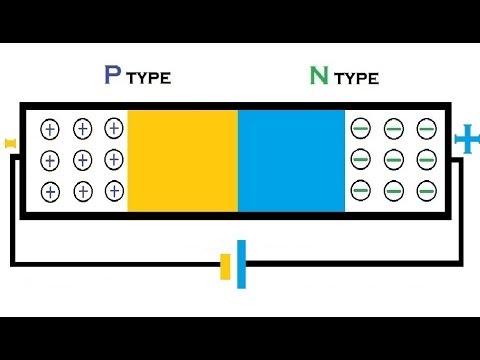
In this video, we will attach metallic contacts at the end of the PN and provide a voltage across it. When we connect P side to Positive and N side to negative, we call it forward biasing.
Class 12 Semiconductors: We cannot imagine our life without computers today. But what makes a computer tick? What's making this technology grow at such an exponential rate? It's all due to semiconductors. As unbelievable as that might sound, altering the properties of semiconductors allows us to build these computers. In this topic, we will explore the world of semiconductors. It's a journey from what semiconductors are all the way to creating building blocks of these computers.
Khan Academy is a nonprofit organization with the mission of providing a free, world-class education for anyone, anywhere. We offer quizzes, questions, instructional videos, and articles on a range of academic subjects, including math, biology, chemistry, physics, history, economics, finance, grammar, preschool learning, and more. We provide teachers with tools and data so they can help their students develop the skills, habits, and mindsets for success in school and beyond. Khan Academy has been translated into dozens of languages, and 15 million people around the globe learn on Khan Academy every month. As a 501(c)(3) nonprofit organization, we would love your help!
Created by Mahesh Shenoy
 0:05:09
How does a forward biased diode work at the molecular level? - Part 2 | Intermediate Electronics
 0:06:50
Forward biasing a PN junction | Class 12 (India) | Physics | Khan Academy
 0:14:50
PN junction Diode Explained | Forward Bias and Reverse Bias
 0:04:11
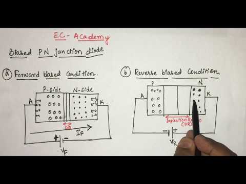
#3 P N junction diode under forward bias and reverse bias Condition || EC Academy
 0:02:13
What is Forward Biased p-n Junction Diode | Electronic Devices & Circuits | Engineering Concepts
 0:14:42
Forward Biased P-N Junction || 2nd Year Physics - Chapter # 18 || 12th Class Physics
 0:03:14
P-N JUNCTION
 0:17:21
Forward Bias (P N Junction Diode) Diode theory & applications (Basic Electronics)
 0:03:28
How does a reverse biased diode work at the molecular level? - Part 3 | Intermediate Electronics
 0:06:37
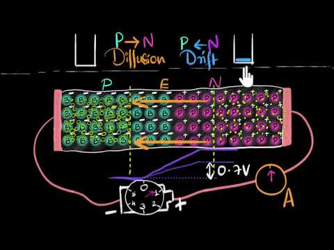
Animation | How a P N junction semiconductor works | forward reverse bias | diffusion drift current
 0:07:07
PN Junction Forward Biasing in tamil
 0:14:06
Diodes - What Are Diodes - PN Junction - Forward Bias - Reverse Bias - Zener Diodes
 0:14:56
🔴 p-n Junction | Forward and Reverse Bias | video in HINDI
 0:02:35
What is p-n Junction Diode | Forward Bias & Reverse Bias | Electronic Devices & Circuits
 0:22:37
Electronic Devices: pn junction - forward and reverse bias
 0:05:45
Reverse biasing a PN junction | Class 12 (India) | Physics | Khan Academy
 0:15:57
56. Forward Bias & Reverse Bias Diode | Semi Conductors | Physics Baba 2.0
 0:08:06
pn junction diode (forward bias) | hindi
 0:24:22
p-n Junction Diode (Part 2) || Forward Bias | Reverse Bias || Semiconductor - 09 || in HINDI
 0:01:00
What is Forward biased PN Junction Diode?
 0:25:01
5.1 Forward and reverse biased PN junctions
 0:00:48
forward bias mode l warm-up match with physics | class12 physics semiconductor | ssp sir
 0:04:58
How to decide either the diode is forward biased or reverse biased ?
 0:13:21
Forward Bias & Reverse Bias | Electronics
Комментарии