filmov
tv
How does a reverse biased diode work at the molecular level? - Part 3 | Intermediate Electronics

Показать описание
Subscribe to the CircuitBread channel for more videos on intermediate electronics!
Table of Contents:
0:00 Introduction
0:15 Difference between forward bias and reverse bias
0:37 How the voltage pulls the carriers away from the depletion region
0:58 Why the depletion region widens under reverse bias
1:06 Energy band diagram of a reverse biased diode
1:54 Breakdown voltage and the avalanche effect
2:47 Summary
CircuitBread is joining the fight to help people more easily learn about and use electronics. With an ever-growing array of equations, tools, and tutorials, we're striving for the best ways to make electronics and electrical engineering topics more accessible to everyone.
Connect with CircuitBread:
 0:03:28
How does a reverse biased diode work at the molecular level? - Part 3 | Intermediate Electronics
 0:05:45
Reverse biasing a PN junction | Class 12 (India) | Physics | Khan Academy
 0:11:40
Photodiodes - (working & why it's reverse biased) | Semiconductors | Physics | Khan Academy
 0:04:58
How to decide either the diode is forward biased or reverse biased ?
 0:14:50
PN junction Diode Explained | Forward Bias and Reverse Bias
 0:03:51
What is Reverse Biased p-n Junction Diode | Electronic Devices & Circuits | Engineering Concepts
 0:06:37
Animation | How a P N junction semiconductor works | forward reverse bias | diffusion drift current
 0:05:09
How does a forward biased diode work at the molecular level? - Part 2 | Intermediate Electronics
 0:04:11
#3 P N junction diode under forward bias and reverse bias Condition || EC Academy
 0:12:17
What Is a Diode?
 0:06:02
What is a Diode? - Forward and Reverse biased diode
 0:02:44
Check For A Forward Biased Or Reverse Biased Diode
 0:02:56
Tricky Diode Forward Reverse Bias Circuits. Part 1
 0:02:33
Reverse biased photodiode is a light level controlled current source component demonstration
 0:13:21
Forward Bias & Reverse Bias | Electronics
 0:04:42
LED Reverse Bias Voltage (VR) Explained
 0:10:26
Reverse Biased P-n Junction || Reverse Biase Characteristics || 2nd Year Physics - Chapter # 18
 0:14:06
Diodes - What Are Diodes - PN Junction - Forward Bias - Reverse Bias - Zener Diodes
 0:04:11
How does it work | Diode forward and reverse bias experiment | Common types of diodes | Alpha Lab
 0:11:50
Forward and reverse current mechanism | Class 12 (India) | Physics | Khan Academy
 0:06:32
PN Junction Reverse Biasing in tamil
 0:00:59
What is Reverse bias PN Junction Diode?
 0:00:41
Reverse biasing of a P-n junction diode Animation
 0:10:03
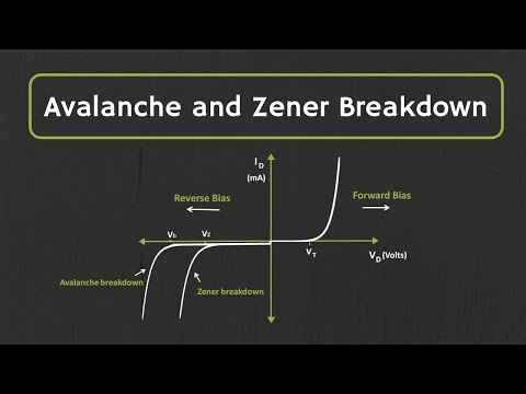
Avalanche Breakdown and Zener Breakdown Effect Explained
Комментарии