filmov
tv
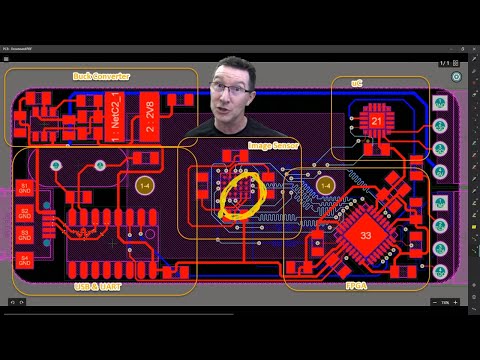
PCB layout guidelines to optimize power supply performance

Показать описание
Download the presentation
This presentation will focus on the fundamental concepts of printed circuit
board (PCB) or printed wiring board (PWB) layout for switch mode power
supplies. These concepts help deliver successful power supply designs
irrespective of power levels and topologies. Also included will be basic
layout parameters influencing the performance of the design, how these
parameters manifest and how to control them. We will explore EMI, thermal
performance and layout examples. This presentation is not only useful for
engineers who are performing the PCB layout activities but also those
engineers who are involved in reviewing the power supply designs and those
who are troubleshooting power supply designs for various issues.
Learn more about UCC28742 flyback controller
Learn more about the UCC24612 SR controller
Learn more about our offline and isolated converter, controller and module portfolio
 1:00:08
PCB layout guidelines to optimize power supply performance
 0:09:27
How To Improve Your PCB Designs (Common Mistakes) - Phil's Lab #18
 0:52:32
How to improve your PCB Layout - Checking Nets
 0:18:54
How GND VIAs Improve Your PCB Layout
 0:27:27
How To Improve Your PCB Layout - Routing & Space
 0:43:41
How To Improve Your PCB Layout - Power Planes
 0:05:51
PCB Design For Beginners: Ugly Tracks Are Noisy
 0:12:47
PCB design best practices: digitally integrated and optimized
 0:06:53
My Top 10 PCB Design Tips
 0:10:40
6 Horribly Common PCB Design Mistakes
 0:42:38
PCB Layout Fundamentals
 0:03:51
PCB Design: Avoiding Common Mistakes & Optimizing Your Process
 0:04:00
Why is 50 OHM impedance used in PCB Layout? | Explained | Eric Bogatin | #HighlightsRF
 0:12:52
Top 5 Beginner PCB Design Mistakes (and how to fix them)
 0:15:47
Optimizing isolated PCB design for EMC
 0:00:53
90° Angles?! Probing LinkedIn AI's PCB Design Guidelines
 0:08:25
PCB Layout Guidelines and Grounding Techniques to Avoid EMI and Crosstalk | Sierra Circuits
 0:04:33
Common PCB designing mistakes to avoid
 0:01:00
Super Pro ESP32 RF PCB Layout: One Minute #PCBDesign Review 05 #electronics #altium
 0:05:19
Up to 255 Amps Power Supply Schematic and PCB Layout | Server Board Design | #HighlightsRF
 0:04:07
How to Design an Automotive PCB Layout for EMI and Thermals
 0:37:29
EEVblog #1323 - PCB Layout Review & Analysis
 0:29:36
Interesting PCB Layout Design Guidelines for Signals above 20Gbps
 0:10:24
Strategies to Optimize Propagation Delay in PCB Design | Sierra Circuits
Комментарии