filmov
tv
Practical RF Hardware and PCB Design Tips - Phil's Lab #19

Показать описание
Some tips for when designing hardware and PCBs with simple RF sections and components. These concepts have aided me well when designing 4-layer embedded systems PCBs.
Topics: critical trace lengths, stackups, controlled impedance traces (microstrip, stripline), impedance discontinuities due to wide pads, clearances, bias tees.
If you're enjoying my content, please consider becoming a patron:
[TIMESTAMPS]
00:00 Introduction
00:27 JLCPCB
00:53 Overview
02:08 Critical length
06:45 Stackup
08:51 Controlled impedance traces
12:34 Impedance discontinuities (pad-to-trace)
14:34 Clearance
15:17 Antenna bias tees
ID: QIBvbJtYjWuHiTG0uCoK
Practical RF Hardware and PCB Design Tips - Phil's Lab #19
Super Pro ESP32 RF PCB Layout: One Minute #PCBDesign Review 05 #electronics #altium
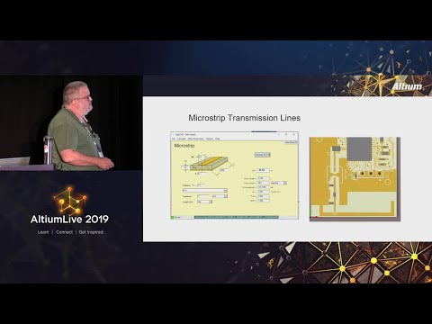
Basic Wireless Design with RF Modules - Wilson
Why is 50 OHM impedance used in PCB Layout? | Explained | Eric Bogatin | #HighlightsRF
6 Horribly Common PCB Design Mistakes
Starting an RF PCB Design
A simple production process for an RF PCB. Is there a video that can be more decompression than this
RF Design in the PCB: Transmission lines (coplanar)
The book every electronics nerd should own #shorts
How does a MOSFET work?
(3) RF and Microwave PCB Design - Stubs - Altium Academy
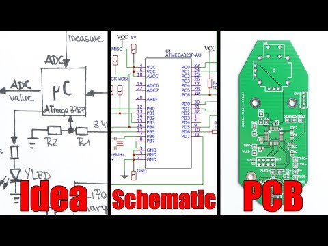
From Idea to Schematic to PCB - How to do it easily!
How to make a LED digital counter using 7- Segment Display
PCB Design For Beginners: Ugly Tracks Are Noisy
RF Transmitter and Receiver Schematics & PCB #electronics #electronicengineering #pcbdesign
Logic Gates Learning Kit #2 - Transistor Demo
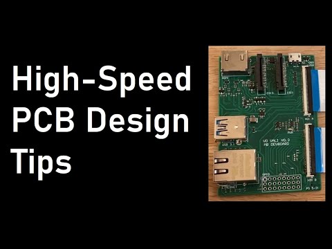
High-Speed PCB Design Tips - Phil's Lab #25
How To Design A PCB With Antenna
RF Design in the PCB: Edge Plating
Which PCB design software is the best 😮 #shorts #startup
final year diploma engineering project #viral #mechanical
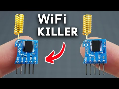
You’ve Never Seen WiFi Like This
How to Quickly Detect Motherboard Short Circuit with the Rosin Dispenser #Shorts
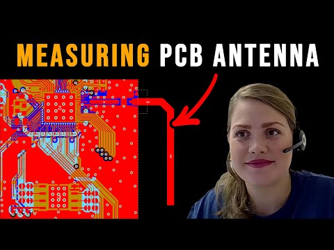
PCB Antenna - How To Design, Measure And Tune
Комментарии
 0:18:46
 0:01:00
 0:49:47
 0:04:00
 0:10:40
 0:17:36
 0:00:53
 0:02:40
 0:00:20
 0:00:53
 0:35:02
 0:11:05
 0:01:00
 0:05:51
 0:00:27
 0:00:23
 0:10:47
 0:01:00
 0:03:01
 0:00:54
 0:00:43
 0:20:43
 0:00:43
 1:35:32