filmov
tv
Easy BGA eMMC PCB Layout With One Simple Trick

Показать описание
How to do layout of an eMMC module with BGA footprint, without the need for multi layer design or via in pad. This video will show you a simple trick that you can use to easily do a PCB layout of a BGA component without any headaches.
 0:12:16
Easy BGA eMMC PCB Layout With One Simple Trick
 0:28:21
BGA PCB Design Tips - Phil's Lab #95
 0:21:00
Your BGA and You | PCB Layout
 0:00:18
Factory Direct Supply ic reball plate BGA Reballing Station Kit for BGA PCB Chip Reballing
 0:03:14
How to Use HDI Stackups during BGA Design
 0:00:51
BGA Reballing Tutorial How To Use Direct Heating Stencil Small stencil holder kit for CPU GPU reball
 0:00:20
bga reballing stencil emmc BGA 153 #shorts
 0:06:57
3 Basic Tricks For EMC Compliant PCB Layout
 0:00:58
BGA Soldering by hand with no template #electronicsrepair #ecurepair #soldering #rework #shorts
 0:43:29
How to do BGA fanout - VIAs & Layers
 0:07:52
Mtk Cpu & eMMC Reballing And Installation
 0:00:29
Remove Emmc B318 BGA221 #shorts
 0:18:51
HOW TO CREATE BGA IN PADS LAYOUT#pads#footprintcreation
 0:00:50
Ic Reballing #mobilerepair #technology
 0:14:11
Fine-Pitch BGA Fanout Altium Designer Walkthrough
 0:02:14
Electronics: Getting started with PCB Layout for BGA Packages (3 Solutions!!)
 0:00:11
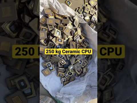
250 kg CPU processors Gold Recovery #ewaste guess How much Gold?
 0:00:16
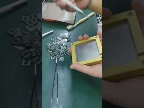
EMMC BGA 186 162 #shorts
 0:00:15
BGA planting fixture fixture: the definitive guide
 0:00:31
Bga Emmc 153 Reball
 0:03:48
How to Create BGA Footprints with the Footprint Wizard
 0:00:21
Power IC - Power Management IC(PMIC)
 0:01:14
Ball Grid Array (BGA) rework - Removal and refit using hot air and flux
 0:17:33
Alternative 4-layer Boards for High Speed PCBs
Комментарии