filmov
tv
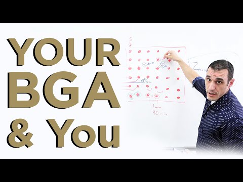
Your BGA and You | PCB Layout

Показать описание
If you're new to PCB Design, the concept of a BGA (or Ball Grid Array) may seem a little overly complicated. But, understanding BGAs helps open the door to mounting a lot of components in a single package. Tech Consultant Zach Peterson lays out everything you need to know to get started with BGAs.
0:00 Intro
1:12 What is a BGA?
2:30 Routing Traces into the Components
4:30 Constructing the Pads
5:58 Routing into the BGA
13:51 An Example BGA
Design guide for BGA fanout and routing:
Don't forget to follow us on social to stay up-to-date on the latest Altium Academy content.
The Altium Academy is an online experience created to bring modern education to PCB Designers and Engineers all across the world. Here you can access a vast library of free training and educational content covering everything from basic design to advanced principles and step-by-step walkthroughs. Join industry legends as they share their career knowledge, review real-life design projects, or learn how to leverage one of Altium's leading design tools. No matter your level of experience, the Altium Academy can help you become a better Designer and Engineer!
About Altium LLC
Altium LLC (ASX:ALU), a global software company based in San Diego, California, is accelerating the pace of innovation through electronics. From individual inventors to multinational corporations, more PCB designers and engineers choose Altium software to design and realize electronics-based products.
#Altium #PCBdesign #AltiumDesigner
 0:21:00
Your BGA and You | PCB Layout
 0:00:16
POV: KSI Laughs At You On BGT .
 0:00:12
POV: you’re in 5th grade music class
 0:00:20
Before you begin your BGA fanout... #pcb #electronicsdesign #shorts
 0:02:54
What if your bga machine's alignment has offset?This video will teach you how to adjust by your...
 0:00:58
BGA Soldering by hand with no template #electronicsrepair #ecurepair #soldering #rework #shorts
 0:00:53
Don't WARP your boards!
 0:05:43
How To Sing Like Your Favorite Artists
![[BGA][TC] Datamania (tpz](https://i.ytimg.com/vi/ZzaRj1ShCxU/hqdefault.jpg) 0:02:18
0:02:18
[BGA][TC] Datamania (tpz Overheat Remix) | by t+pazolite 【EZ2ON REBOOT : R】
 0:00:28
installing a Ryzen CPU into an Intel motherboard #shorts
 0:00:15
How to Replace Laptop CPU | Laptop Processor@macnitesh #laptop #CPU
 0:00:15
You been Running thru my mind all day 🏃🏽♀️💨
 0:00:28
Pokemon Card Grading | Who do I choose? BGS/CGC/PSA
 0:00:16
How to Check Graphics Card Details in Laptop | Graphics Card Details Short Cut#macnitesh#2023shorts
 0:00:34
barbie blind bag! 💖 #blindbag #blindbags #craft #diy #barbie #papersquishy #papercraft #asmr
 0:00:30
Let’s buy another blind bag that i made from my shop that i also made using the money that i made
 0:00:21
This will get you BANNED in Pokémon GO
 0:00:12
Reballing Like a Pro in 12 Seconds!
 0:00:15
How to Connect Monitor to Laptop For VGA Cable#macnitesh#2023shorts#monitor
 0:00:56
Going through my middle-high school makeup bag 💄#part1 #2000s #throwback #asmr #nostalgia
 0:00:16
Unlock Soldering Precision: Desoldering Braid and Essential Tools for BGA Repair
 0:00:21
How to Play APT on Soprano Recorder (and Why You Should)
 0:00:38
3 Pokémon GO exploits that became TOP strategies
 0:00:31
How To Make Custom Trigger Stops For *FREE*... #Shorts
Комментарии