filmov
tv
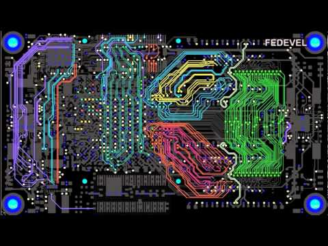
Watch routing PCB Layout with DDR3 & High Speed Interfaces

Показать описание
Thank you very much to Blaine for the music!
 0:01:43
Watch routing PCB Layout with DDR3 & High Speed Interfaces
 0:06:58
Introducing AI Auto-Layout: a new way to route PCBs
 0:17:56
Aesthetic PCB Design Tips - Phil's Lab #84
 0:27:27
How To Improve Your PCB Layout - Routing & Space
 0:12:52
Top 5 Beginner PCB Design Mistakes (and how to fix them)
 0:10:40
6 Horribly Common PCB Design Mistakes
 0:06:53
My Top 10 PCB Design Tips
 0:10:10
From Rats Nest to a complete PCB layout in 10 steps // Designing a LoRa-GPS tracker in KiCad
 0:59:21
Overcoming DDR Routing Challenges With Advanced PCB Design and DFM Practices | Sierra Circuits
 0:09:27
How To Improve Your PCB Designs (Common Mistakes) - Phil's Lab #18
 0:15:07
QFN Layout and Routing - Tips & Tricks
 0:10:56
Basic KiCad 2-Layer PCB Routing Demonstration
 0:10:47
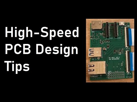
High-Speed PCB Design Tips - Phil's Lab #25
 0:14:43
When to Use an Autorouter in PCB Design
 0:04:24
Circuit Routing Tips for PCB Designers
 0:01:09
How to Route in Altium Designer 17 using ActiveRoute - PCB Design Software
 0:14:01
Voltage Regulator Layout on a 2-Layer Board | PCB Routing Tips
 0:25:06
Switching Regulator PCB Design - Phil's Lab #60
 0:00:43
PCB - Route - Auto Router
 1:03:20
Ground in PCB Layout - Separate or Not Separate? (with Rick Hartley)
 0:26:38
FPGA/SoC + DDR PCB Design Tips - Phil's Lab #59
 0:28:21
BGA PCB Design Tips - Phil's Lab #95
 0:13:16
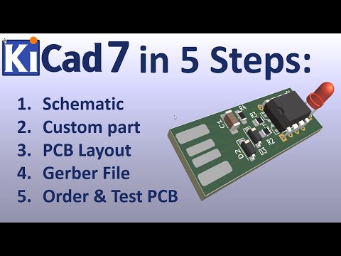
KiCAD 7 PCB Layout in 5 steps
 1:40:06
KiCad 6 STM32 PCB Design Full Tutorial - Phil's Lab #65
Комментарии