filmov
tv
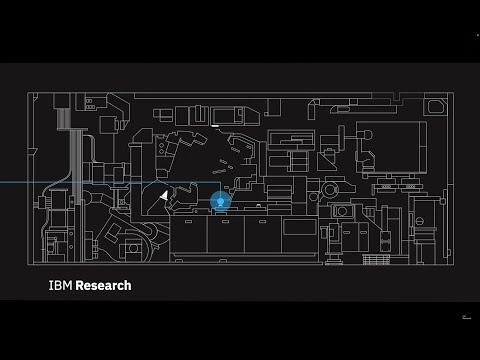
How EUV lithography works

Показать описание
Over the years, semiconductors have drastically shrunk in size. Computers used to take up entire rooms, and now we have machines more powerful than the computers that guided NASA to the Moon sitting on our wrist. To find ways to make chips even smaller and more powerful, we have to work with new tools. Back in 2015, IBM Research argued that the future of chipmaking would require EUV lithography machines, which are now becoming the industry standard for chips with transistors just three or four nanometers wide. Learn more about what EUV lithography is, and how it relates to a centuries-old printing technique.
#EUV #eda #semiconductors #chiplets
#EUV #eda #semiconductors #chiplets
 0:01:37
How EUV lithography works
 0:17:20
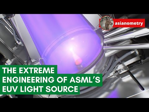
The Extreme Engineering of ASML’s EUV Light Source
 0:01:39
TRUMPF EUV lithography – This all happens in one second
 0:04:20
Behind this Door: Learn about EUV, Intel’s Most Precise, Complex Machine
 0:18:40
Why The World Relies On ASML For Machines That Print Chips
 0:01:39
Unveiling High NA EUV | ASML
 0:18:51
How Extreme Ultraviolet Lithography works | Part 1/3
 0:05:47
Samsung Semiconductor Explains Photo Lithography and EUV in 5 Minutes
 0:06:54
How An EUV Light Source Works
 0:02:08
New ASML High-NA EUV Lithography Chipmaker Costs $380 Million
 0:13:36
How Carl Zeiss Crafts Optics for a $150 Million EUV Machine
 0:03:51
Intel Adds ASML’s First High NA EUV Tool to Oregon Factory
 0:19:14
ASML's High-NA EUV Lithography: A 2024 Update
 0:16:15
How an ASML Lithography Machine Moves a Wafer
 0:15:45
You Didn’t Build your PC… This Did. - ASML Cymer Tour
 0:01:09
ASML in 1 Minute | ASML
 0:24:28
“The Decision of the Century”: Choosing EUV Lithography
 0:16:34
ASML's High-NA and Hyper-NA EUV: An Update
 0:07:44
‘Semiconductor Manufacturing Process’ Explained | 'All About Semiconductor' by Samsung Sem...
 0:14:17
EUV’s Most Difficult Challenge
 0:15:19
What ASML Has Next After EUV
 0:14:52
How ASML Builds a $150 Million EUV Machine
 0:53:09
ASML's Secret: An exclusive view from inside the global semiconductor giant | VPRO Documentary
 0:27:48
How are Microchips Made? 🖥️🛠️ CPU Manufacturing Process Steps
Комментарии