filmov
tv
EUV’s Most Difficult Challenge

Показать описание
ASML and its partners had to overcome many challenges in order to make EUV lithography a reality.
For instance, in a previous video I talked about the EUV light source and its double-shot technique. But while challenging, that had not been considered one of EUV's dealbreaking issues.
A greater struggle was how to achieve a zero defect rate for the EUV photomask, or reticle. I will use the two terms interchangeably here.
The EUV reticle contains the chip design. Any defects on the reticle larger than a certain size will show up on the printed wafers themselves. So in order for it to work, it must be truly perfect.
In this video, we look at how ASML managed to overcome this ultra-critical aspect of the technology.
Links:
 0:14:17
EUV’s Most Difficult Challenge
 0:04:20
Behind this Door: Learn about EUV, Intel’s Most Precise, Complex Machine
 0:10:06
EUV : Grand Challenges : Part 1
 0:00:44
Understanding EUV: The Magic of Extreme Ultraviolet Lithography
 0:01:37
How EUV lithography works
 0:13:36
How Carl Zeiss Crafts Optics for a $150 Million EUV Machine
 0:02:01
EUV Enablement: Solving Defect Challenges
 0:24:28
“The Decision of the Century”: Choosing EUV Lithography
 0:22:23
EUV Photoresists: The Next Generation?
 0:18:40
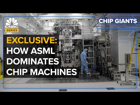
Why The World Relies On ASML For Machines That Print Chips
 0:15:19
What ASML Has Next After EUV
 0:16:34
ASML's High-NA and Hyper-NA EUV: An Update
 0:00:12
How much? #mechanichumor #snapon #toolbox
 0:20:43
High-NA EUV Progress And Problems
 0:06:37
USA vs China Military Power Comparison 2025 | China vs USA Military Power 2025
 0:25:33
Japan’s EUV Failure
 0:00:46
China's military robotic wolves unveiled at Airshow China 2024
 0:12:37
EUV : Achilles heel of scaling
 0:16:52
Russia Shocks the Tech World: Develops its own EUV lithography machine to Rival ASML!
 0:07:37
EUV cannot improve the yield rate, what is the impact on ASML
 0:00:12
easy to remove mirror cover tricks.
 0:00:23
How to reset the tire pressure indicator light on your car
 0:16:15
How an ASML Lithography Machine Moves a Wafer
 0:00:32
Supercruz VS HEAVY rain!
Комментарии