filmov
tv
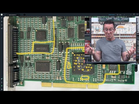
EEVblog 1512 - Why Bypass Your PCB Like THIS?

Показать описание
Why add bypass capacitors on a PCB like THIS?
Answering a Twitter question:
Support the EEVblog on:
Buy anything through that link and Dave gets a commission at no cost to you.
Donate With Bitcoin & Other Crypto Currencies!
#ElectronicsCreators #Bypassing #pcb
Answering a Twitter question:
Support the EEVblog on:
Buy anything through that link and Dave gets a commission at no cost to you.
Donate With Bitcoin & Other Crypto Currencies!
#ElectronicsCreators #Bypassing #pcb
 0:19:02
EEVblog 1512 - Why Bypass Your PCB Like THIS?
 0:19:57
EEVblog 1511 - Solar Analytics System FAIL! (+ Dave gets ZAPPED!)
 0:29:57
EEVblog 1441 - Electric Buses are NOT a SCAM (Adam Something)
 0:08:12
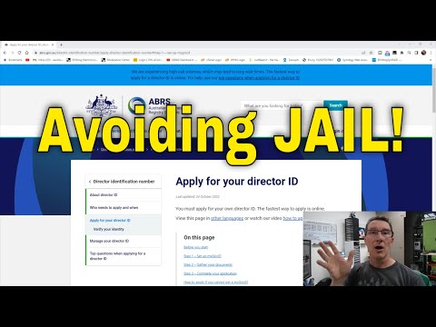
Avoiding JAIL! - On Hold With The Government - MyGovID
 0:39:59
EEVblog 1498 - TransPod Fluxjet Hyperloop $550M Boondoggle!
 0:33:36
LIVE new EEVblog product teardown
 0:23:59
EEVblog #1353 - WHY Are These Pins Shorted?
 0:05:35
Dumpster Diving LG TV
 0:21:33
Enphase vs Tigo | Watch this REAL TEST | Which one is better? Microinverter vs Optimizer
 0:02:16
Output coupling capacitors in dual-supply op amp circuits (2 Solutions!!)
 0:03:32
HD PVR 2 - Capture Old Consoles (SNES, SEGA, N64, Gamecube, etc.)
 0:06:35
How to make a Li-ion battery for e-bike using dead laptop batteries.
 0:59:08
Inside the Microsoft FPGA based configurable cloud
 0:12:36
#449 INA217 Instrumentation Amplifier Microphone Preamp
 0:08:29
AC - Example Emitter Bias Bypass
 0:45:58
Sony Trinitron KV1913 Repair and EOL
Комментарии