filmov
tv
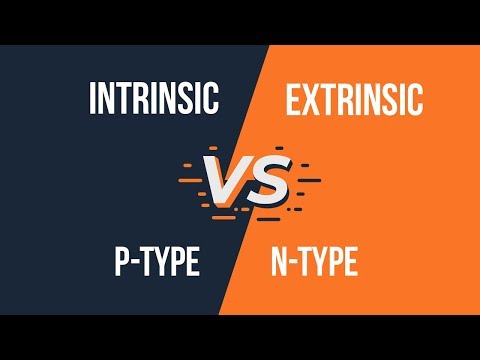
Types of Semiconductor Materials | Intrinsic & Extrinsic Semiconductor | Engineering Funda

Показать описание
Types of Semiconductor Materials in Electronic Devices is explained with the following timecodes:
0:00 - Types of Semiconductor Materials - Electronic Devices
0:43 - Intrinsic Semiconductor
5:13 - Extrinsic Semiconductor
8:44 - N-type Semiconductor
10:04 - P-type Semiconductor
The following points are covered in this video:
0. Electronic Devices
1. Types of Semiconductor Materials
2. Intrinsic Semiconductor
3. Extrinsic Semiconductor
4. N-type Semiconductor
5. P-type Semiconductor
Chapter-wise detailed Syllabus of the Electronic Devices - EDC Course is as follows:
Energy Bands and Classification of Solid Materials, Types of Semiconductor Materials, Drift Current and Diffusion Current, Mass Action Law, Examples of Semiconductor Materials, Examples of Drift Current and Diffusion Current, Examples of Conductivity and Resistivity, Einstein Relation in Semiconductor, Examples of Einstein Relation in Semiconductor, Fermi Dirac Distribution in Semiconductor, Electron Concentration in Conduction band and Holes Concentration in Valance Band, Intrinsic Concentration in Semiconductor, Drift Velocity and Free Velocity, Fermi Energy Level in Intrinsic Semiconductor, Fermi Energy Level in Extrinsic Semiconductor, Hall Effect in Semiconductor, Examples of Hall Effect in Semiconductor, Energy & Wavelength for Generation and Recombination, Examples of Energy & Wavelength for Generation and Recombination, Generation and recombination due to uniform illumination, Examples of Generation and recombination, Energy Band Diagram, Examples of Energy Band Diagram, Continuity Equation, Direct Bandgap and Indirect Bandgap Semiconductor.
PN Junction in Equilibrium, Energy Band Diagram of PN Junction, Cut in Voltage of PN Junction, Electric Field of PN Junction, Depletion Width of PN Junction, Examples of PN Junction, PN Junction under forward bias, PN Junction under reverse bias, Ideal Diode & Practical Diode, Diode Ratings, Diode Testing and Diode Quality Verification, Effect of Temperature in PN Junction, Examples of Diode Circuits, PN Junction Capacitance, Examples of PN Junction Capacitance, PN Junction Switching Characteristics.
LED - Light Emitting Diode, Examples of LED, Varactor Diode, Tunnel Diode, Examples of Tunnel Diode, Photo Diode, Solar Cell, Examples of Solar Cell.
BJT Parameters under Equilibrium, BJT Operation Regions, BJT Applications & BJT Base Width, BJT in Active Region, BJT Carrier Distributions in Different Modes, Ebers Moll Model of BJT, Early Effect, Common Base Configuration of BJT, Common Emitter Configuration of BJT, Punch Through in BJT, Examples of BJT.
MOSCAP, MOS Capacitor, Ideal MOSCAP, Flat Band Voltage in MOSCAP, MOSCAP under External Bias, MOSCAP under Accumulation Mode, MOSCAP under Depletion Mode, MOSCAP under Inversion Mode, Threshold Voltage of MOSCAP, Inversion Charge of MOSCAP, CV Characteristics of MOSCAP, Examples of MOSCAP.
MOSFET, IV Characteristics of MOSFET, Channel Length Modulation of MOSFET, Small Signal Model of MOSFET, Transconductance and Drain Resistance of MOSFET, Body Effect in MOSFET, Examples of MOSFET, Examples of IC Technology.
Use of Function Generator in MULTISIM, VI Characteristics of PN Junction Diode in MULTISIM, Zener Diode Characteristics in MULTISIM, Half wave Rectifier in MULTISIM, Full wave Rectifier in MULTISIM, Bridge Rectifier in MULTISIM, Logic GATEs in MULTISIM, Clipper Circuits in MULTISIM, Common Emitter Characteristics of BJT in MULTISIM, Frequency Response of Common Emitter Amplifier in MULTISIM, FET Characteristics in MULTISIM
Engineering Funda channel is all about Engineering and Technology. Here this video is a part of Basic Electronics/ Electronic Devices /EDC.
#Semiconductor #ElectronicDevices #BasicElectronics @EngineeringFunda
Комментарии
 0:05:12
 0:12:44
 0:12:23
 0:04:53
 0:06:32
 0:10:50
 0:04:46
 0:04:25
 0:53:17
 0:07:44
 0:08:23
 0:00:05
 0:13:13
 0:08:59
 0:00:11
 0:08:39
 0:04:52
 0:00:11
 0:13:56
 0:15:50
 0:05:49
 0:04:11
 0:03:48
 0:00:22