filmov
tv
Semiconductor Packaging - ASSEMBLY PROCESS FLOW

Показать описание
This is a learning video about semiconductor packaging process flow. This is a good starting point for beginners. - Watch Learn 'N Play
UPDATE 8/15/2022: FIXED ENGLISH SUBTITLE. PLEASE USE SUBTITLE IF YOU CANNOT UNDERSTAND MY ACCENT (PARDON MY ACCENT AND MY GRAMMAR TOO :) )
UPDATE 8/15/2022: FIXED ENGLISH SUBTITLE. PLEASE USE SUBTITLE IF YOU CANNOT UNDERSTAND MY ACCENT (PARDON MY ACCENT AND MY GRAMMAR TOO :) )
Semiconductor Packaging - ASSEMBLY PROCESS FLOW
Semiconductor Packaging Explained | 'All About Semiconductor' by Samsung Electronics
A Brief History of Semiconductor Packaging
‘Semiconductor Manufacturing Process’ Explained | 'All About Semiconductor' by Samsung Sem...
[Eng Sub] Semiconductor Package Overall: Structure, Process
Semiconductor production process explained
Inside Micron Taiwan’s Semiconductor Factory | Taiwan’s Mega Factories EP1
Electronic Device Assembly & Packing Process From Start To Finish.
Amkor Technology, Pioneers of the OSAT Industry
Making Memory Chips – Semiconductor manufacturing process
Packaging Part 5 - Manufacturing process
5223 Semiconductor Packaging -- Manufacturing -- Assembly
[Eng Sub] Wafer Bumping Process: Solder bump, Cu pillar bump, UBM
Nordson ASYMTEK: The NexJet System - Flip Chip Underfill
Introduction to Wafer-Level Packaging
Semiconductor Packaging Performance – High-Tech Industry Process Experience
Tiwei Wei: Semiconductor Packaging, Heat Transfer, and Assembly
THE SEMICONDUCTOR SUPPLY CHAIN - A BRIEF OVERVIEW
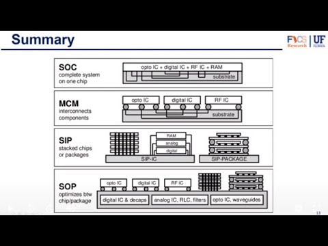
Packaging Part 2 - Introduction to IC Packaging
[Eng Sub] Substrate - Flipchip Substrate Manufacturing Process, Core, Build-up, ABF
Semiconductor Packaging - PACKAGE STRUCTURE
Packaging Part 6 - Wafer to Panel Level Packaging
DIE ATTACH PROCESS
WIRE BONDING (PART 1)
Комментарии
 0:26:31
 0:02:48
 0:18:31
 0:07:44
![[Eng Sub] Semiconductor](https://i.ytimg.com/vi/_SM4KqQR8A4/hqdefault.jpg) 0:03:28
0:03:28
 0:02:05
 0:23:01
 0:01:24
 0:46:22
 0:04:21
 0:19:04
 0:04:49
![[Eng Sub] Wafer](https://i.ytimg.com/vi/VLwqssWjRMU/hqdefault.jpg) 0:04:28
0:04:28
 0:00:34
 0:02:45
 0:02:11
 0:01:46
 0:03:48
 0:15:55
![[Eng Sub] Substrate](https://i.ytimg.com/vi/HiJHMBPcOyg/hqdefault.jpg) 0:05:54
0:05:54
 0:07:16
 0:18:44
 0:09:26
 0:15:53