filmov
tv
Are my Circuits ILLEGAL to use?!

Показать описание
In this video we will be having a look at three buck/boost converter boards built around the same IC, the TPS6302. One of these boards you can get for cheap from Asia. The other two ones are DIY designs I made myself. And the main question for this video is whether they pass EMC guidelines which are super important when you want to sell your board. We will be testing conductive and radiated EMC. And at the end I will show you how you can fix EMC problems of such boards. Let's get started!
Websites that were shown/used during the video:
Thanks to the Würth Elektronik for supporting this video.
0:00 EMC Problems?
1:32 Intro
1:54 EMC Measurements at Home?
2:56 Conductive EMC Tests
4:38 Conductive EMC Results
5:29 Radiated EMC Tests & Results
6:32 Legal to Sell?
7:02 Fixing EMC Problems
10:03 Verdict
 0:10:42
Are my Circuits ILLEGAL to use?!
 0:07:57
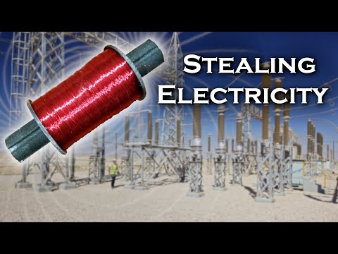
Stealing Electricity (The safe way)
 0:00:39
Replacing 100 amp main breaker and removing wire on illegal generator backfeed outlet. Raphael Simon
 0:04:15
Worst Electrical Mistake You Can Make - Backfeeding Generators
 0:00:12
Is this legal or illegal? #f123 #f12023 #f1game
 0:00:36
illegal PC components #shorts
 0:00:27
This small difference LOST me HALF A SECOND...
 0:00:22
Found a illegal generator back feed! We disconnected it.
 0:00:58
Is It Illegal To Install Outlets Upside Down? #shorts
 0:00:43
Illegal HAM Radio Button? (20% off Ham Radio course in pinned comment) #civtac #gun #demolitionranch
 0:05:11
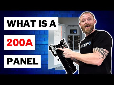
How Do I Know if My Panel is 200 Amps? (What Makes a 200 Amp Panel 200 Amps)
 0:22:01
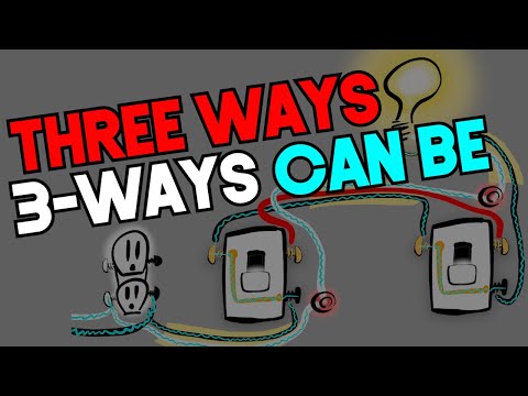
THREE WAYS 3-WAYS CAN BE (3way Switch Wiring - ILLEGAL AND LEGAL METHODS)
 0:01:58
What is a Double Tapped Circuit Breaker?
 0:04:21
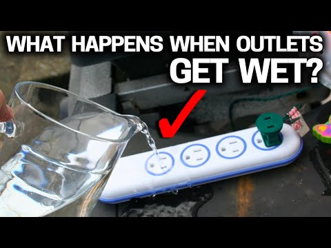
What REALLY HAPPENS WHEN YOU SPILL WATER in an OUTLET?
 0:01:01
Is this Old Fuse Panel Illegal? #thisoldhouse #edison #hustleandgrind
 0:00:34
This is just about as sketchy as it gets! Illegal generator back feed. #electrician #simonelectric
 0:05:12
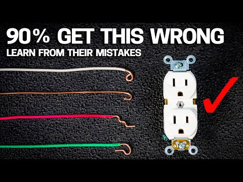
BEWARE Of These 3 Common Wiring Mistakes On Outlets & Switches
 0:11:44
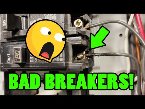
How to Tell if a Breaker is Bad
 0:00:47
Do you think my EV is illegal?
 0:10:21
This Illegal Car Mod Just Changed the Game
 0:02:05
Illegal Neutral to Ground connection @ Air Conditioner disconnect box
 0:10:05
This Illegal Mod Will Make Your Car Run Better
 0:01:00
Boxing Lessons With Floyd Mayweather #Shorts
 0:14:58
Making Intelligence with Basic Switch
Комментарии