filmov
tv
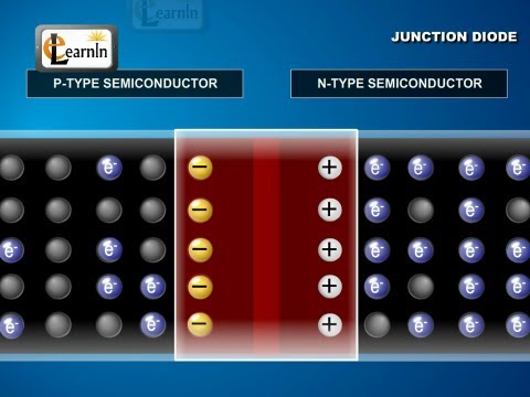
Depletion Region

Показать описание
 0:05:03
How does a diode work - the PN Junction (with animation) | Intermediate Electronics
 0:01:04
Depletion Region
 0:14:50
PN junction Diode Explained | Forward Bias and Reverse Bias
 0:09:59
PN Junction Introduction
 0:02:44
Formation and Properties of Junction Diode - Physics
 0:05:09
How does a forward biased diode work at the molecular level? - Part 2 | Intermediate Electronics
 0:03:14
P-N JUNCTION
 0:10:06
The PN junction | Class 12 (India) | Physics | Khan Academy
 0:10:49
Diffusion, drift & barrier voltage | Class 12 (India) | Physics | Khan Academy
 0:07:54
How does a Diode Work? A Simple Explanation | How Diodes Work | Electrical4U
 0:13:38
The depletion region
 0:05:03
Introduction to P-N Junction Diode and Formation of Depletion Region - Basic Electronics
 0:07:22
depletion region in transistor
 0:41:43
104N. PN Junction, Depletion Region, Diode Equation
 0:02:23
What is Potential Barrier | Formation of Depletion Region | Electronic Devices and Circuits
 0:04:43
Depletion Layer Thickness
 0:10:22
L3 2 2pn Depletion Region Width and Charge
 0:11:30
How transistor works? | Depletion layer | Diffusion | Drift
 0:00:45
Formation of Depletion layer
 0:12:59
#depletionregion #barrierpotential Diode | Depletion Region | Barrier Potential | The PrimeGuide
 0:00:32
The increase in the width of the depletion region in a p-n junction diode is due to
 0:04:43
FORMATION OF DEPLETION REGION BY SAURABH
 0:01:13
In a p-n junction the depletion region is 400 nm wide and electric field of 5 × 10^5Vm^-1 exists......
 0:04:50
What are the Different Regions of Operation for a FET? | Intermediate Electronics
Комментарии